| Jan 15, 2019 |
Researchers develop novel photonic crystal actuator materials(Nanowerk News) Photonic crystals (PCs) have attracted enormous research interest due to their unique light manipulation property. The superwettability of the PC endows materials of many novel applications in high-efficient sensing, catalysts, detection and etc. |
| In the CAS key laboratory of bio-inspired materials and interface Sciences, Technical Institute of Physics and Chemistry, a series of important progress has been made in the preparation and application of superwetting PCs. For example, the effect of substrate wettability plays a great role on the morphology and molecular assembly of latex particles. |
| Combining the droplet-template with interface assembly, series of anisotropic PCs with flower-shape and bread-shape was developed. A PC microarray with good optical waveguide behavior was prepared from sandwich substrate with special wettability. A novel PC pattern was developed by electrowetting -etching approach. An outdoor carbon dot optical coating with anti-counterfeiting properties and anti-optical structure film, and a shape memory PCs were prepared (ACS Nano, "A Hydrophilic/Hydrophobic Janus Inverse-Opal Actuator via Gradient Infiltration"). |
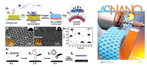 |
| Figure 1. Prepared Janus photonic crystal film and cover picture. (Image: WANG Jingxia) |
| Actuating materials have become a novel and promising research topic owing to its potential applications in intelligent robots and micro-biological dynamic monitoring. In nature, many organisms respond to water in the environment or solvent for actuation. Typically, the seed dispersal units of pinecones, wheat awns and seedpods remain in their closed state when on the tree or under a wet environment, and they are able to open and release the seeds as they dry out. |
| Inspired by these smart organisms, various stimulus actuators have been fabricated from a passive-active bilayer structure, with responsive materials as the active layer combined with the passive material as the substrate. However, the bilayer actuator is difficult to be frequently used due to the poor adhesion of the two-layer structure. |
| To solve this problem, a single chemical composition gradient driving material has emerged. In the previous work, single-material polyionic liquid inverse opal PC actuator was developed based on the gradient de-wetting process. |
| Subsequently, a solvent-responsive actuator with continuous bending/debending behavior was prepared by excessively penetrating the liquid crystal monomer into the colloidal crystal template and then photopolymerization. |
| Recently, Professor WANG Jingxia at Technical Institute of Physics and Chemistry, Chinese Academy of Sciences, together with Professor CHEN Bo from Hunan Normal University have jointly developed a Janus-type poly (ionic liquid-methyl methacrylate) copolymer inverse opal PC film by gradient filling method (Figure 1). |
| The upper surface of the actuator is a hydrophilic polyionic liquid, and the lower surface is enriched with hydrophobic polymethyl methacrylate. |
| The different properties of the two sides of the prepared sample are mainly due to the phase separation caused by the different polymerization behavior of ionic liquid and methyl methacrylate during the photopolymerization process, resulting in a gradient distribution of the chemical composition along the thickness direction of the film. |
 |
| Figure 2. The structural color change and the actuating process during the actuating of the prepared Janus PC film can draw the mechanical engineer motion. (Image: WANG Jingxia) |
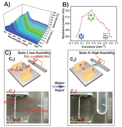
| The Janus property of the prepared film has obvious directional bending behavior upon water vapor, and the bending angle is close to 144° within four seconds, accompanied by a bright structural color change. |
| The actuating behavior of the film can be adjusted by the chemical composition of the film, the size of the pores, and the type of solvent. The directional drive performance of the sample was simulated by COMSOL, the as-prepared actuator was used for the drive an engineer via using a single film (size: 12 mm x 3 mm x 20 µm) (Figure 2). |
| This research work provides an important insight for the development of novel PC-based optical devices. |
| Source: Chinese Academy of Sciences |
|
Subscribe to a free copy of one of our daily Nanowerk Newsletter Email Digests with a compilation of all of the day's news. |

