| Jan 17, 2019 |
Light connects two worlds on a single chip(Nanowerk News) For the first time, researchers of the University of Twente succeeded in connecting two parts of an electronics chip using an on-chip optical link. A light connection can, for example, be a safe way of connecting a high-power part and digital control circuitry on one chip, without a direct electrical link. |
| Until now, however, an optical link was not possible using standard silicon chip technology. Vishal Agarwal, a UT PhD student, managed to do so. He realized a very small optocoupler circuit that delivers a data rate of Megabits per second in an energy-efficient way ("Optocoupling in CMOS"). |
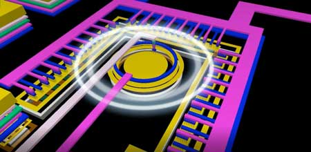 |
| Artist impression of the optocoupler, the round structure is the detector (Single Photon Avalanche Diode), the light source (Avalanche Mode LED) has the shape of a horse shoe. (Image: University of Twente) |
| Using light, it is possible to isolate one part of a chip of another: the two different worlds will be able to communicate, but there is no electrical connection. In ‘smart power’ chips, the high-power part can be isolated from the digital control circuits. This isolation guarantees safe operation in application areas like medical electronics and automotive. |
| A so-called ‘optocoupler’ is used for this, but until now, this is a bulky device, separated from the actual chip. The dream, having an on-chip optocoupler, has now been realized by Vishal Agarwal. His optocoupler can be integrated with the electronics using standard chip technology (CMOS). It is about 0,008 square millimeter in size and consumes minimal energy. |
Avalanche |
| Integrating a light source and a light detector on a chip, is not trivial at all. In general, special materials will be needed that simply can’t be introduced in the CMOS process. Silicium is not a good light source by itself. A silicon LED on a chip would emit some infrared light with low efficiency, while a silicon detector doesn’t work well with infrared light. This is not a good starting point at all, for a good connection. |
| Previous research, however, by UT PhD student Satadal Dutta, proved that better results can be obtained by connecting the silicon LED ‘the wrong way’. What will happen, is an avalanche effect, resulting in the emission of visible light. In the same way, a light detector can be made at which a single photon can induce an avalanche. The result: an efficient optical connection. |
Efficient design |
| The principle worked, now for Agarwal the challenge was to design an electronic circuit that controls the LED and the detector in the best way, optimizing for energy consumption, speed, and use of space on the chip. For example: what is the voltage needed for operating the ‘Avalanche Mode LED’ (AMLED) and the ‘Single Photon Avalanche Diode’ (SPAD) in the most efficient way, resulting in a good connection without wasting light? How to position the light source and light detector on the chip, for the highest efficiency? |
| In his thesis, Agarwal comes up with an optocoupler that can be fully integrated in CMOS, with a data rate of about 1 Megabit per second and minimum energy consumption. Although for many applications, the is already an acceptable data rate, it can be increased at least tenfold, according to Agarwal. |
| The research has been done in two Electrical Engineering groups of the University of Twente: Integrated Circuit Design (Digital Society Institute), led by Bram Nauta and Integrated Devices and Systems (MESA+ Institute) led by Prof Jurriaan Schmitz. In this way, the underlying physics of the connection and the actual design could be combined in the best possible way. |
| Source: University of Twente |
|
Subscribe to a free copy of one of our daily Nanowerk Newsletter Email Digests with a compilation of all of the day's news. |

