| Jan 21, 2019 |
New material to push the boundaries of silicon-based electronics(Nanowerk News) The electronics market is growing constantly and so is the demand for increasingly compact and efficient power electronic systems. The predominant electronic components based on silicon will in foreseeable future no longer be able to meet the increasing industrial requirements. |
| This is why scientists from the university of Freiburg, the Sustainability Center Freiburg and the Fraunhofer-Gesellschaft have joined forces in order to explore a new material structure that may be better suited for future power electronics. |
| The recently launched project »Research of Functional Semiconductor Structures for Energy Efficient Power Electronics« (in short »Power Electronics 2020+«) researches the novel semiconductor material scandium aluminum nitride (ScAlN). Prof. Dr. Oliver Ambacher, director of Fraunhofer IAF and professor of power electronics at the Department of Sustainable Systems Engineering (INATECH) of the university of Freiburg, coordinates the supra-regional collaboration. |
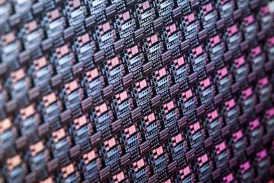 |
| The image shows a processed GaN wafer. (Image: Fraunhofer IAF) |
| Three key factors are responsible for the strong growth of the electronics market: the automation and digitalization of the industry as well as the increasing awareness of ecological responsibility and sustainable processes. Power consumption can only be lowered if electronic systems become more more energy- and resource-efficient the same time they become more powerful. |
Silicon Technology Reaches its Physical Limit |
| Up to date, silicon dominates the electronics industry. With its relative low cost and an almost perfect crystal structure, silicon has become a particularly successful semiconductor material, also because its bandgap allows for both a good charge carrier concentration and velocity as well as a good dielectric strength. |
| However, silicon electronics gradually reaches its physical limit. Especially with regard to the required power density and compactness, silicon power electronic components are insufficient. |
Innovative Material Composition for More Power and Efficiency |
| The limitations of silicon technology have already been overcome by the use of gallium nitride (GaN) as a semiconductor in power electronics. GaN performs better in conditions of high voltages, high temperatures and fast switching frequencies compared to silicon. This goes hand in hand with significantly higher energy efficiency—with numerous energy-consuming applications, this means a significant reduction in energy consumption. |
| Fraunhofer IAF has been researching GaN as a semiconductor material for electronic components and systems for many years. With the help of industrial partners, the results of these research work has already been put to commercial use. |
| The scientists of the project »Power Electronics 2020+« will go even further in order to once more enhance the energy efficiency and durability of the next generation of electronic systems. For this purpose, a different and novel material will be used: scandium aluminum nitride (ScAlN). |
First Components Based on ScAlN |
| ScAlN is a piezoelectric semiconductor material with a high dielectric strength which is largely unexplored worldwide with regard of its usability in microelectronic applications. »The fact that scandium aluminum nitride is especially well suited for power electronic components, due to its physical properties, has already been proven«, explains Dr.-Ing. Michael Mikulla, project manager on the part of Fraunhofer IAF. |
| The aim of the project is to grow lattice-matched ScAlN on a GaN layer and to use the resulting heterostructures to process transistors with high current carrying capacity. »Functional semiconductor structures based on materials with a large bandgap, such as scandium aluminum nitride and gallium nitride, allow for transistors with very high voltages and currents. These devices reach a higher power density per chip surface as well as higher switching speeds and higher operating temperatures. |
| This is synonymous with lower switching losses, higher energy efficiency and more compact systems«, adds Prof. Dr. Oliver Ambacher, director of Fraunhofer IAF. »By combining both materials, GaN and ScAlN, we want to double the maximal possible output power of our devices while at the same time significantly lowering the energy demand«, says Mikulla. |
Pioneering Work in Materials Research |
| One of the biggest challenges of the project is crystal growth, considering that there exsist structure neither growth recipes nor empirical values for this material, yet. The project team needs to develop these during the next months in order to reach reproducible results and to produce layer structures that can successfully be used for power electronic applications. |
Specialist Collaboration and Knowledge Transfer Between Freiburg and Erlangen |
| The research project will be conducted in close cooperation between the university of Freiburg, the Fraunhofer Institute for Applied Solid State Physics IAF, the Sustainability Center Freiburg as well as the Fraunhofer Institure for Integrated Systems and Device Technology IISB in Erlangen, which is a member of the High-Performance Center for Electronic Systems in Erlangen. |
| This new form of collaboration between university research and application-oriented development shall serve as a role model for future project cooperation. »On the one hand, this model facilitates the cooperation with companies through the prompt transfer of results from basic research to application-oriented development. |
| On the other hand, it opens up synergies between two technically complementary Fraunhofer Centers from two different regions and thus improves both their offers for potential customers of the semiconductor industry«, reasons Prof. Ambacher. |
| Source: Fraunhofer Institute for Applied Solid State Physics |
|
Subscribe to a free copy of one of our daily Nanowerk Newsletter Email Digests with a compilation of all of the day's news. |

