| Feb 14, 2019 |
Scientists develop direct-write quantum calligraphy in monolayer semiconductors(Nanowerk News) Scientists at the U.S. Naval Research Laboratory (NRL) and the Air Force Research Laboratory (AFRL) have developed a way to directly write quantum light sources, which emit a single photon of light at a time, into monolayer semiconductors such as tungsten diselenide (WSe2) (ACS Nano, "Quantum Calligraphy: Writing Single-Photon Emitters in a Two-Dimensional Materials Platform"). |
| Single photon emitters (SPEs), or quantum emitters, are key components in a wide range of nascent quantum-based technologies, including computing, secure communications, sensing and metrology. |
| In contrast with conventional light emitting diodes which emit billions of photons simultaneously to form a steady stream of light, an ideal SPE generates exactly one photon on demand, with each photon indistinguishable from another. These characteristics are essential for photon-based quantum technologies under development. |
| In addition, such capabilities should be realized in a material platform which enables precise, repeatable placement of SPEs in a fully scalable fashion compatible with existing semiconductor chip manufacturing. |
| NRL scientists used an atomic force microscope (AFM) to create nanoscale depressions or indents in a single monolayer of WSe2 on a polymer film substrate. A highly localized strain field is produced around the nano-indent which creates the single photon emitter state in the WSe2. Time correlated measurements performed at AFRL of this light emission confirmed the true single photon nature of these states. These emitters are bright, producing high rates of single photons, and spectrally stable, key requirements for emerging applications. |
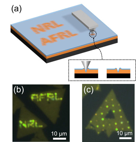 |
| (a) Illustration showing an AFM tip indenting the TMD/polymer structure to introduce local strain. (b) Patterned single photon emission in WSe2 induced by AFM indentation of the letters 'NRL' and 'AFRL'. (c) AFM indents produce single photon emitter 'ornaments' on a monolayer WSe2 'Christmas tree.' (U.S. Naval Research Laboratory) |
| "This quantum calligraphy allows deterministic placement and real time design of arbitrary patterns of SPEs for facile coupling with photonic waveguides, cavities and plasmonic structures," said Berend Jonker, Ph.D., senior scientist and principal investigator. "Our results also indicate that a nano-imprinting approach will be effective in creating large arrays or patterns of quantum emitters for wafer scale manufacturing of quantum photonic systems." |
| Dr. Matthew Rosenberger, lead author of the study, points out the importance of this discovery stating, "In addition to enabling versatile placement of SPEs, these results present a general methodology for imparting strain into two dimensional (2D) materials with nanometer-scale precision, providing an invaluable tool for further investigations and future applications of strain engineering of 2D devices." |
| The results of this study pave the way for the use of 2D materials as solid state hosts for single photon emitters in applications relevant to the Department of Defense (DoD) mission, such as secure communications, sensing and quantum computation. Such applications enable communication between distant DoD forces which is not vulnerable to eavesdropping or decryption, an essential requirement to insure the safety of the warfighter. |
| Quantum computation on a chip provides onboard capability to rapidly analyze very large data sets acquired by sensor arrays, so that the entire data set does not have to be transmitted, reducing bandwidth requirements. |
| Source: U.S. Naval Research Laboratory |
|
Subscribe to a free copy of one of our daily Nanowerk Newsletter Email Digests with a compilation of all of the day's news. |

