| Mar 04, 2019 |
Step right up for bigger 2D sheets(Nanowerk News) Very small steps make a big difference to researchers who want to create large wafers of two-dimensional material. |
| Atom-sized steps in a substrate provide the means for 2D crystals growing in a chemical vapor furnace to come together in perfect rank. Scientists have recently observed this phenomenon, and now a Rice University group has an idea why it works. |
| Rice materials theorist Boris Yakobson and researcher Ksenia Bets led the construction of simulations that show atom-sized steps on a growth surface, or substrate, have the remarkable ability to keep monolayer crystal islands in alignment as they grow. |
| If the conditions are right, the islands join into a larger crystal without the grain boundaries so characteristic of 2D materials like graphene grown via chemical vapor deposition (CVD). That preserves their electronic perfection and characteristics, which differ depending on the material. |
| The Rice theory appears in the American Chemical Society journal Nano Letters ("How the Complementarity at Vicinal Steps Enables Growth of 2D Monocrystals"). |
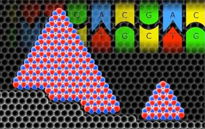 |
| Rice University researchers determined complementarity between growing hexagonal boron nitride crystals and a stepped substrate mimics the complementarity found in strands of DNA. The Rice theory supports experiments that have produced large, oriented wafers. (Image: Ksenia Bets/Rice University) |
| The investigation focused on hexagonal boron nitride (h-BN), aka white graphene, a crystal often grown via CVD. Crystals nucleate at various places on a perfectly flat substrate material and not necessarily in alignment with each other. |
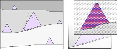
| However, recent experiments have demonstrated that growth on vicinal substrates – surfaces that appear flat but actually have sparse, atomically small steps – can align the crystals and help them merge into a single, uniform structure, as reported on arXiv. A co-author of that report and leader of the Korean team, Feng Ding, is an alumnus of the Yakobson lab and a current adjunct professor at Rice. |
| But the experimentalists do not show how it works as, Yakobson said, the steps are known to meander and be somewhat misaligned. |
| “I like to compare the mechanism to a ‘digital filter,’ here offered by the discrete nature of atomic lattices,” he said. “The analog curve that, with its slopes, describes a meandering step is ‘sampled and digitized’ by the very grid of constituent atomic rows, breaking the curve into straight 1D-terrace segments. The slope doesn’t help, but it doesn’t hurt. Surprisingly, the match can be good; like a well-designed house on a hill, it stands straight. |
| “The theory is simple, though it took a lot of hard work to calculate and confirm the complementarity matching between the metal template and the h-BN, almost like for A-G-T-C pairs in strands of DNA,” Yakobson said. |
| It was unclear why the crystals merged into one so well until simulations by Bets, with the help of co-author and Rice graduate student Nitant Gupta, showed how h-BN “islands” remain aligned while nucleating along visibly curved steps. |
| “A vicinal surface has steps that are slightly misaligned within the flat area,” Bets said. “It has large terraces, but on occasion there will be one-atom-high steps. The trick by the experimentalists was to align these vicinal steps in one direction.” |
| In chemical vapor deposition, a hot gas of the atoms that will form the material are flowed into the chamber, where they settle on the substrate and nucleate crystals. h-BN atoms on a vicinal surface prefer to settle in the crook of the steps. |
| “They have this nice corner where the atoms will have more neighbors, which makes them happier,” Bets said. “They try to align to the steps and grow from there. |
| “But from a physics point of view, it’s impossible to have a perfect, atomically flat step,” she said. “Sooner or later, there will be small indentations, or kinks. We found that at the atomic scale, these kinks in the steps don’t prevent h-BN from aligning if their dimensions are complementary to the h-BN structure. In fact, they help to ensure co-orientation of the islands.” |
 |
| Complementarity between the energies of atoms forming hexagonal boron nitride and a metal substrate lead to uniform wafers of 2D materials in a chemical vapor deposition furnace. The theoretical confirmation by Rice University scientists shows how growing crystals of the material use the steps in a vicinal substrate to stay oriented, which allows them to join into larger crystals. (Image: Ksenia Bets/Rice University) |
| Because the steps the Rice lab modeled are 1.27 angstroms deep (an angstrom is one-billionth of a meter), the growing crystals have little trouble surmounting the boundary. “Those steps are smaller than the bond distance between the atoms,” Bets said. “If they were larger, like two angstroms or higher, it would be more of a natural barrier, so the parameters have to be adjusted carefully.” |
| Two growing islands that approach each other zip together seamlessly, according to the simulations. Similarly, cracks that appear along steps easily heal because the bonds between the atoms are strong enough to overcome the small distance. |
| Any path toward large-scale growth of 2D materials is worth pursuing for an army of applications, according to the researchers. 2D materials like conductive graphene, insulating h-BN and semiconducting transition metal dichalcogenides are all the focus of intense scrutiny by researchers around the world. The Rice researchers hope their theoretical models will point the way toward large crystals of many kinds. |
| Source: By Mike Williams, Rice University |
|
Subscribe to a free copy of one of our daily Nanowerk Newsletter Email Digests with a compilation of all of the day's news. |

