| Mar 18, 2019 |
Mass manufacturing of metasurfaces(Nanowerk News) The mass production of flat optical devices with sub-wavelength structures could soon be a reality, thanks to a metasurface fabrication technique developed by researchers at A*STAR (Optics Express, " Demonstration of color display metasurfaces via immersion lithography on a 12-inch silicon wafer"). |
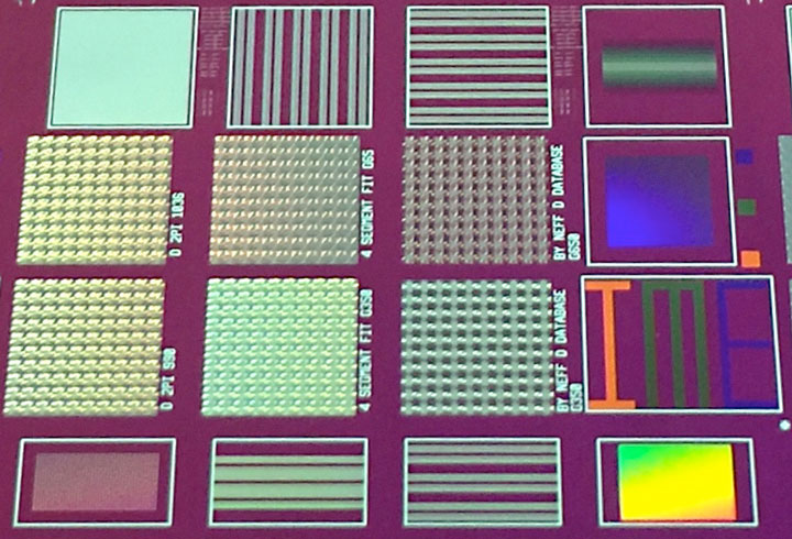 |
| The metasurface's nano-pillar arrays displaying the letters I, M and E in red, green and blue, respectively. (© The Optical Society) (click on image to enlarge) |
| Metasurfaces are synthetic, two-dimensional materials covered in tiny individual shapes with sizes and spacings smaller than the wavelengths of visible light. These ‘sub-wavelength’ structures enable scientists to precisely control the propagating shape, or wavefront, of light beams. As such, metasurfaces show promise for many applications from high-resolution imaging and color printing to controlling light polarization. Mass production of metasurfaces, however, has proven challenging, limited by the complexity of realizing such precise patterns. |
| Now, Ting Hu and his colleagues at A*STAR’s Institute of Microelectronics (IME) have developed a method of building silicon-based metasurfaces by introducing existing techniques from semiconductor fabrication. Their new metasurface design can produce high-resolution red-green-blue (RGB) color displays. |
| Until now, metasurfaces have mainly been fabricated via electron beam lithography (EBL), which is not applicable to mass production, as Hu explains: |
| “With EBL, the focused electron beam moves slowly, step by step, across the metasurface substrate. Metasurfaces with millions — possibly billions — of elements require a very long time to be patterned via EBL. We desired a faster and more efficient way of patternation.” |
| Hu and the team based their technique on ‘immersion lithography’, which has long been used to etch patterns on to electronic components. With multiple exposures, complex patterns can be built up. The researchers used ultraviolet-based (UV) lithography for initial patternation on to silicon substrates, followed by plasma etching to form the designs in small pixel blocks that were assembled into a 12-inch display surface (see image). |
| “Our UV lithography tool is a scanner, which can pattern a whole 12 inch wafer with designed devices within half an hour,” says Hu. “We designed the physical dimensions of the nano-pillar arrays of the metasurface to accurately display colors, with fantastic results, for example displaying the letters I, M and E in red, green and blue respectively.” |
| Hu and the team hope to optimize their design and improve the etching process to minimize losses induced by light scattering and defects in the nano-structure arrays. They are also making efforts to realize flat, lightweight ‘meta-lenses’ and dot projectors with potential uses in facial recognition technologies. |
| Source: A*STAR |
|
Subscribe to a free copy of one of our daily Nanowerk Newsletter Email Digests with a compilation of all of the day's news. |

