| Mar 22, 2019 |
Optical tweezers combine with X-rays to enable analysis of crystals in liquids(Nanowerk News) Understanding how chemical reactions happen on tiny crystals in liquid solutions is central to a variety of fields, including materials synthesis and heterogeneous catalysis, but obtaining such an understanding requires that scientists observe reactions as they occur. |
| By using coherent X-ray diffraction techniques, scientists can measure the exterior shape of and strain in nanocrystalline materials with a high degree of precision. However, carrying out such measurements requires precise control of the position and angles of the tiny crystal with respect to the incoming X-ray beam. Traditionally, this has meant adhering or gluing the crystal to a surface, which in turn strains the crystal, thus altering its structure and potentially affecting reactivity. |
| Now, scientists at the U.S. Department of Energy's (DOE) Argonne National Laboratory and the University of Chicago have developed a new technique that combines the power of nanoscale "tractor beams" with high-powered X-rays, enabling them to position and manipulate crystals in solution that are not in contact with substrates (PNAS, "Three-dimensional optical trapping and orientation of microparticles for coherent X-ray diffraction imaging"). |
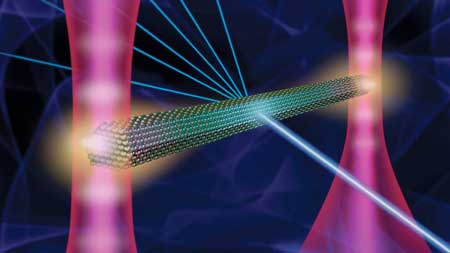 |
| Scientists have found a way to use "optical tweezers" by employing lasers, a mirror and a light modulator to anchor a crystal in solution. The "tweezers" have made it possible to conduct X-ray diffraction measurements of a crystal suspended in solution. (Image: Robert Horn/Argonne National Laboratory) |
| The tractor beam technique is known as "optical tweezers," which was also coincidentally awarded the 2018 Nobel Prize in Physics, because it allows samples to be manipulated using only light. |
| While ordinary optical tweezers involve a single focused laser beam, the holographic optical tweezers used in the study involve lasers precisely modified with a spatial light modulator. These lasers are reflected off a mirror to create an interference pattern of "hotspots" that are both more localized than a simply focused laser beam and have rapidly reconfigurable locations. The electric field gradient of these focused hotspots attracts the polarizable crystal and holds it in place. |
| With a pair of tweezers engaged -- each at one end of the crystal -- the Argonne scientists could manipulate the semiconductor microcrystal in three dimensions with high precision in the presence of a liquid solution and without exposing it to other surfaces. |
| "Usually, when people look at microcrystals using X-ray diffraction, they're glued onto a sample holder, which causes a distortion," said Argonne distinguished fellow Linda Young, a corresponding author on the study. "But now, with optical tweezers, you can capture a single particle in its native state in solution and watch its structural evolution. In principle, you can add reactants, capture dissolution or reaction and monitor changes at an atomic level." |
| By gaining the ability to manipulate the sample using only light, Young and her colleagues were able to take advantage of the coherent X-rays produced by Argonne's Advanced Photon Source (APS), a DOE Office of Science User Facility. Using a technique called Bragg coherent diffraction imaging (CDI), the researchers were able to examine the crystal's structure under real conditions and from a number of different angles. |
| By pairing optical tweezers with Bragg CDI, scientists now have a new way to explore materials in liquid media, explained Brookhaven National Laboratory (BNL) scientist Yuan Gao, the first author of the study. "Our discovery comes from a combination of different techniques -- including pairing lasers with the coherent beam from the APS," he said. "To make the experiment work, we needed the nanofabrication technique at the Center for Nanoscale Materials to make the sample cell as well." The Center for Nanoscale Materials (CNM) is also a DOE Office of Science User Facility. |
| According to Young, the technique might be useful for a wide range of future studies, including nucleation and crystal growth. "Typically, people look at isolated nanocrystalline samples in air or in vacuum. We wanted to be able control such objects in the liquid phase. For example, we wanted to be able to watch catalysis or crystallization unfold in real time with the precision that is afforded by X-ray crystallography," she said. |
| Gao pointed to the stability afforded by the optical tweezers as a primary advantage for future coherent X-ray experiments. "Coherent diffraction is very sensitive to position and orientation of the sample, and this experiment demonstrated the possibilities of this new technique," he said. Because of the stability of the technique, investigators were able to obtain coherent diffraction data, which allowed them to reconstruct the sample with sub-nanometer accuracy, revealing sub-nanometer scale defects and grain boundaries within the ostensibly crystalline ZnO microcrystal. |
| "As we look toward the upgrade of the APS, which will increase the brightness of the X-ray beams by orders of magnitude, these measurements will be much faster and provide even more exciting insight into how samples change in time," added Ross Harder, an Argonne physicist at the APS who is an author on the paper. |
| Eventually, the researchers would like to extend the technique to capture the ultrafast evolution of the crystal when it is excited by a laser pulse, said University of Chicago chemistry professor Norbert Scherer, another author of the paper. "This is the first step in achieving our larger ambition, which is to visualize the time-dependent structural dynamics of how the lattice changes," he said. |
| To carry out the experiment, the researchers relied on the creation of microfluidic components at CNM. Electrodynamics simulations were also carried out at CNM's Carbon high-performance computing cluster. University of Chicago researchers contributed their expertise on the holographic optical tweezer technique. |
| Source: Argonne National Laboratory |
|
Subscribe to a free copy of one of our daily Nanowerk Newsletter Email Digests with a compilation of all of the day's news. |

