| Apr 10, 2019 |
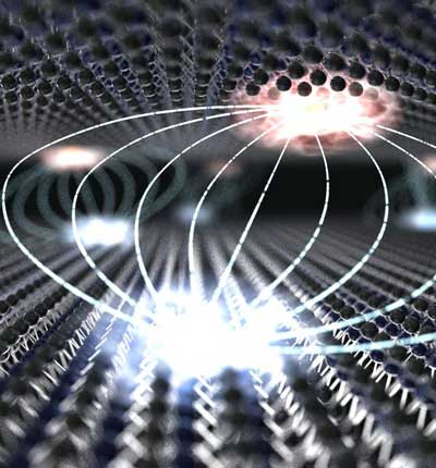
A long-distance relationship in femtoseconds(Nanowerk News) Modern electronics relies on ultrafast charge motion on ever shorter length scales. Physicists from Regensburg and Gothenburg have now succeeded in resolving a key quantum motion of electrons in atomically thin crystals on the time scale of a single oscillation cycle of light. They directly observe, how the electron in a bound electron-hole pair jumps from one atomic layer to the next, creating a pair of charge carriers in a long-distance relationship, a so-called "interlayer exciton". |
| The results have been published in the journal Nature Materials ("Ultrafast transition between exciton phases in van der Waals heterostructures"). |
 |
| Artistic representation of an interlayer exciton in a layered structure of monolayer transition metal dichalcogenides. The electron (blue) and the hole (red) interact across the atomic distance. (Illustration: Brad Baxley) |
| In order to make electronics more powerful, nowadays circuits are becoming ever more compact. Here, the limit is the atomic length scale. Novel, layered crystals of so-called transition metal dichalcogenides, which can be thinned down to a few atomic layers, promise ultimately thin components such as solar cells and transistors. However, charge carriers behave very unconventionally in only two dimensions. |
| For example, if an electron is excited by absorbing light in a transition metal dichalcogenide, it leaves behind a hole at its original location. Electron and hole can form a bound pair, an exciton. The negatively charged electron orbits the positively charged hole in analogy to an electron in the hydrogen atom orbiting the nucleus. Because of the strong attraction between electrons and holes, these excitons are also stable at room temperature. |
| For important applications, such as solar cells, however, electrons and holes need to be spatially separated. This is achieved by stacking two different dichalcogenides on top of each other. Physicists from Regensburg led by Professors Rupert Huber, Tobias Korn, John Lupton and Christian Schüller have now observed this charge separation of excitons across only two atomically thin layers in collaboration with Professor Ermin Malic's group at Chalmers University in Sweden. |
| They excited electrons by ultrashort light pulses creating excitons selectively only in one of the two layers. If these excitons remain within this layer, they are very short-lived, because electrons and holes recombine very rapidly with the electron returning to its initial position. |
| In a layered sample structure, on the other hand, the electron can also jump into the adjacent layer – a spatially separated, so-called interlayer exciton forms. |
| "Since the layers are atomically thin, the electron still feels the hole’s presence, so they can continue to interact across the layer," explains Fabian Mooshammer, PhD student and co-author of the study. |
| Due to the spatial separation, however, it takes much longer for the electron to return to its initial position. This significantly longer lifetime is only one of the reasons why interlayer excitons have caused a lot of excitement in recent years, both in fundamental research and in optoelectronics. |
| The scientists were able to observe the behavior of these interlayer excitons during and after their formation. They used a home-built super slow-motion camera to study processes taking place within a few femtoseconds – the millionth part of a billionth of a second. |
| "For the first time worldwide, we observed the formation process of an interlayer exciton and measured how strongly electrons and holes remain bound," says Philipp Merkl, first author of the publication. |
| In addition, the researchers were able to systematically influence the dynamics of the formation process. To this end, they used another special feature of the layered heterostructures: they twisted the two layers with respect to each other. This changes the electronic and optical properties of the resulting structure, which in turn governs the charge transfer. |
| These new findings represent an important milestone in the development of novel, custom-tailored layered structures and could pave the way for a new generation of ultimately compact and efficient electronics, optoelectronics and information technologies. |
| Source: Universität Regensburg |
|
Subscribe to a free copy of one of our daily Nanowerk Newsletter Email Digests with a compilation of all of the day's news. |

