| Jun 27, 2019 |
Bursts of light shape walls between waves of charge(Nanowerk News) To better store data, scientists need ways to change a material’s properties suddenly. For example, they want a material that can go from insulator to conductor and back again. |
| Now, they devised a surprisingly simple way of flipping a material from one state into another, and back again, with flashes of light (Science Advances, "Ultrafast manipulation of mirror domain walls in a charge density wave"). A single light pulse turns thin sheets of tantalum disulfide from its original (alpha) state into a mixture of alpha and beta states. Domain walls separate the two states. A second pulse of light dissolves the walls, and the material returns to its original state. |
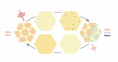 |
| Single pulses of laser light switch tantalum disulfide (large yellow hexagons) from one state to another and back again. Clockwise from left: A single light pulse turns the material from its initial alpha (red) state into a mixture of alpha and beta (blue) states. The states are separated by domain walls (right). A second light pulse dissolves the domain walls, and the material returns to its original state. Switches like this could lead to new forms of data storage. (Image: MIT) |
| The material’s new properties result from emerging patterns of electrons. Scientists can use these changes in electron charge distributions to build novel computers and more. Today’s computers manipulate the magnetic spin for data storage. This work shows that scientists could use the electron charge density to create pathways for new electronic devices. |
| Switching the configurations of electrons in a way that changes a material’s properties is key to information storage, processing, and transmission. Scientists have demonstrated new ultrafast laser pulse techniques to change the charge ripples that exist in a material. The ripples, known as charge density waves, result from the quantum interactions of electrons and lattice vibrations. |
| The long-range electron patterning creates “super-lattice” signatures, which can be measured with electron and X-ray scattering. Scientists studied ultrathin tantalum disulfide, which consists of layers of tantalum atoms sandwiched by sulfur atoms. |
| Some of the electron charge normally associated with the locations of the atoms bunches up like peaks and troughs of waves, in positions and angles that are not completely aligned with the atomic structure. These electron density waves have two possible orientations, which the researchers switched using short bursts of laser light. When the light is strong enough, photo-induced defects in the system induce one orientation or the other at different locations. |
| Eventually the oriented regions meet at boundary walls. These walls are expected to have different properties than the bulk material and might, for example, be used to switch the material from an insulator to a conductor at low temperature. To remove these walls, the scientists used a less intense pulse of light to return the material to a single orientation. |
| The researchers plan to investigate the use of photoexcitation to perform ultrafast domain wall engineering and thus control materials properties in a switchable way on extremely short time scales, possibly leading to new quantum level electronic devices. |
| Source: U.S. Department of Energy, Office of Science |
|
Subscribe to a free copy of one of our daily Nanowerk Newsletter Email Digests with a compilation of all of the day's news. |

