| Sep 13, 2019 |
New topological insulator reroutes photonic 'traffic' on the fly(Nanowerk News) Topological insulators are a game-changing class of materials; charged particles can flow freely on their edges and route themselves around defects, but can't pass through their interiors. This perfect surface conduction holds promise for fast and efficient electronic circuits, though engineers must contend with the fact that the interiors of such materials are effectively wasted space. |
| Now, researchers from the University of Pennsylvania, where topological insulators were first discovered in 2005, have shown a way to fulfill that promise in a field where physical space is at an even bigger premium: photonics. They have shown, for the first time, a way for a topological insulator to make use of its entire footprint. |
| By using photons instead of electrons, photonic chips promise even faster data transfer speeds and information-dense applications, but the components necessary for building them remain considerably larger than their electronic counterparts, due to the lack of efficient data-routing architecture. |
| A photonic topological insulator with edges that can be redefined on the fly, however, would help solve the footprint problem. Being able to route these "roads" around one another as needed means the entire interior bulk could be used to efficiently build data links. |
 |
| The researchers' chip features a tessellated grid of oval rings. By "pumping" individual rings with an external laser, they are able dynamically redefine the path photons take. (Image: University of Pennsylvania) |
| Researchers at Penn's School of Engineering and Applied Science have built and tested such a device for the first time, publishing their findings in the journal Science ("Non-Hermitian topological light steering"). |
| "This could have a big impact on large-information capacity applications, like 5G, or even 6G, cellphone networks," says Liang Feng, assistant professor in Penn Engineering's Departments of Materials Science and Engineering and Electrical and Systems Engineering. |
| "We think this may be the first practical application of topological insulators," he says. |
| Feng led the study along with graduate student Han Zhao, a member of his lab. Fellow lab members Xingdu Qiao, Tianwei Wu and Bikashkali Midya, along with Stefano Longhi, professor at the Polytechnic University of Milan in Italy, also contributed to the research. |
| The data centers that form the backbone of communication networks route calls, texts, email attachments and streaming movies to and between millions of cellular devices. But as the amount of data flowing through these data centers increases, so does the need for high-capacity data routing that can keep up with the demand. |
| Switching from electrons to photons would speed up this process for the upcoming information explosion, but engineers must first design a whole new library of devices for getting those photons from input to output without mixing them up and losing them in the process. |
| Advances in data-processing speed in electronics have relied on making their core components smaller and smaller, but photonics researchers have needed to take a different approach. |
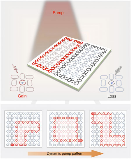 |
| The researchers' chip features a tessellated grid of oval rings. By "pumping" individual rings with an external laser, they are able to dynamically redefine the path photons take. (Image: University of Pennsylvania) |
| Feng, Zhao and their colleagues set out to maximize the complexity of photonic waveguides -- the prescribed paths individual photons take on their way from input to output -- on a given chip. |
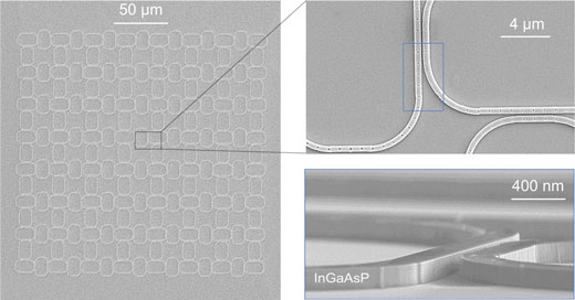
| The researchers' prototype photonic chip is roughly 250 microns squared, and features a tessellated grid of oval rings. By "pumping" the chip with an external laser, targeted to alter the photonic properties of individual rings, they are able to alter which of those rings constitute the boundaries of a waveguide. |
| The result is a reconfigurable topological insulator. By changing the pumping patterns, photons headed in different directions can be routed around each other, allowing photons from multiple data packets to travel through the chip simultaneously, like a complicated highway interchange. |
| "We can define the edges such that photons can go from any input port to any output port, or even to multiple outputs at once," Feng says. "That means the ports-to-footprint ratio is at least two orders of magnitude greater than current state-of-the-art photonic routers and switches." |
| Increased efficiency and speed is not the only advantage of the researchers' approach. |
| "Our system is also robust against unexpected defects," Zhao says. "If one of the rings is damaged by a grain of dust, for example, that damage is just making a new set of edges that we can send photons along." |
| Since the system requires an off-chip laser source to redefine the shape of the waveguides, the researcher's system is not yet small enough to be useful for data centers or other commercial applications. Next steps for the team will be to establish a fast reconfiguring scheme in an integrated fashion. |
| Source: University of Pennsylvania |
|
Subscribe to a free copy of one of our daily Nanowerk Newsletter Email Digests with a compilation of all of the day's news. |

