| Sep 16, 2019 |
Light and sound in silicon chips: The slower the better(Nanowerk News) Integrated circuits in silicon enable our digital era. The capabilities of electronic circuits have been extended even further with the introduction of photonics: components for the generation, guiding and detection of light. Together, electronics and photonics support entire systems for data communication and processing, all on a chip. However, there are certain things that even electrical and optical signals can't do simply because they move too fast. |
| Sometimes moving slowly is actually better, according to Prof. Avi Zadok of Bar-Ilan University's Faculty of Engineering and Institute of Nanotechnology and Advanced Materials. "Important signal processing tasks, such as the precise selection of frequency channels, require that data is delayed over time scales of tens of nano-seconds. Given the fast speed of light, optical waves propagate over many meters within these timeframes. One cannot accommodate such path lengths in a silicon chip. It is unrealistic. In this race, fast doesn't necessarily win." |
| The problem, in fact, is a rather old one. Analog electronic circuits have been facing similar challenges in signal processing for sixty years. An excellent solution was found in the form of acoustics: A signal of interest is converted from the electrical domain to the form of an acoustic wave. The speed of sound, of course, is slower than that of light by a factor of 100,000. Acoustic waves acquire the necessary delays over tens of micro-meters instead of meters. Such path lengths are easily accommodated on-chip. Following propagation, the delayed signal can be converted back to electronics. |
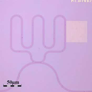 |
| Top-view microscope image of a surface acoustic wave photonic device in silicon on insulator. A grating of gold stripes (right) is used to drive acoustic waves, which then affect light in standard waveguides. (© Nature Communications) |
| In a new work published in the journal Nature Communications ("Surface acoustic wave photonic devices in silicon on insulator"), Zadok and co-workers carry over this principle to silicon-photonic circuits. |
| "There are several difficulties with introducing acoustic waves to silicon chips," says doctoral student Dvir Munk, of Bar-Ilan University, who participated in the study. "The standard layer structure used for silicon photonics is called silicon on insulator. While this structure guides light very effectively, it cannot confine and guide sound waves. Instead, acoustic waves just leak away." Due to this difficulty, previous works that combine light and sound waves in silicon do not involve the standard layer structure. Alternatively, hybrid integration of additional, nonstandard materials was necessary. |
| "That first challenge can be overcome by using acoustic waves that propagate at the upper surface of the silicon chip," continues Munk. "These surface acoustic waves do not leak down as quickly. Here, however, there is another issue: Generation of acoustic waves usually relies on piezo-electric crystals. These crystals expand when a voltage is applied to them. Unfortunately, this physical effect does not exist in silicon, and we much prefer to avoid introducing additional materials to the device." |
| As an alternative, students Munk, Moshe Katzman and coworkers relied on the illumination of metals. "Incoming light carries the signal of interest," explains Katzman. "It irradiates a metal pattern on the chip. The metals expand and contract, and strain the silicon surface below. With proper design, that initial strain can drive surface acoustic waves. In turn, the acoustic waves pass across standard optical waveguides in the same chip. Light in those waveguides is affected by the surface waves. In this way, the signal of interest is converted from one optical wave to another via acoustics. In the meantime, significant delay is accumulated within very short reach." |
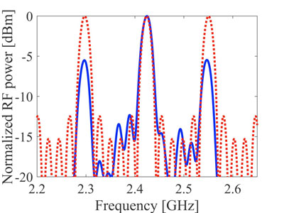 |
| Measured frequency response of a narrow radio-frequency filter, realized using light and sound waves in a silicon chip. Blue: Experimental results. Red: Designed response. (© Nature Communications) |
| The concept combines light and sound in standard silicon with no suspension of membranes or use of piezo-electric crystals. Acoustic frequencies up to 8 GHz are reached, however the concept is scalable to 100 GHz. The working principle is applicable to any substrate, not only silicon. Applications are presented as well: the concept is used in narrowband filters of input radio-frequency signals. The highly selective filters make use of 40 nanosecond long delays. "Rather than use five meters of waveguide, we achieve this delay within 150 microns," says Munk. |
| Prof. Zadok summarizes: "Acoustics is a missing dimension in silicon chips because acoustics can complete specific tasks that are difficult to do with electronics and optics alone. For the first time we have added this dimension to the standard silicon photonics platform. The concept combines the communication and bandwidth offered by light with the selective processing of sound waves." |
| One potential application of such devices is in future cellular networks, widely known as 5G. Digital electronics alone might not be enough to support the signal processing requirements in such networks. Light and sound devices might do the trick. |
| Source: Bar-Ilan University |
|
Subscribe to a free copy of one of our daily Nanowerk Newsletter Email Digests with a compilation of all of the day's news. |

