| Sep 24, 2019 |
Highly sensitive nanowire diode converts microwaves to electricity(Nanowerk News) In preparation for the commencement of the true IoT era, energy harvesting technologies, which transform the minute sources of energy in the surrounding environment into electricity, have come under the spotlight in recent years as means for creating sensor networks that function without batteries. One such example reuses as electricity the low-power radio waves (microwaves), ubiquitous in open space, that are emitted from mobile phone base stations, for use in communications. Equipment used in generating electricity from ambient radio waves consists of a radio wave power generating element, which includes an antenna for collecting radio waves and a rectifying element (diode) that rectifies the radio waves (figure 1). |
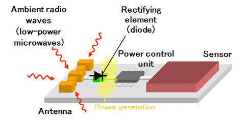 |
| Figure 1. Overview Diagram of Power Generation using Ambient Radio Waves. A small-scale antenna receives radio waves (microwaves) that are emitted in the surrounding environment, such as from mobile phone base stations, and uses them as an energy source to power sensors. As the electricity conversion element, highly sensitive diodes are required to enable low-power radio waves to be rectified. |
| The responsiveness (sensitivity) of a diode to microwaves largely depends on the steepness of rectification characteristics and on diode size (capacity). Generally, Schottky barrier diodes, which utilize the rectification occurring at the junction formed between a metal and a semiconductor, are used as the diodes for power conversion. Due to rectification characteristics becoming slow at extremely low voltages and the size of elements being larger than several micrometers (µm), however, sensitivity to low-power microwaves weaker than microwatts (µW) was insufficient, and it was difficult to convert ambient radio waves into electricity. This led to a demand for diodes with increased sensitivity. |
| The Japan Science and Technology Agency (JST), Fujitsu Limited, and the Tokyo Metropolitan University today announced that they developed a highly sensitive rectifying element in the form of a nanowire backward diode, which can covert low-power microwaves into electricity. Through JST's Strategic Basic Research Programs, the technology was developed by researchers led by Kenichi Kawaguchi of Fujitsu Limited and Professor Michihiko Suhara of the Tokyo Metropolitan University. The new technology is expected to play a role in harvesting energy from radio waves in the environment, in which electricity is generated from ambient radio waves, such as those emitted from mobile phone base stations. |
| To facilitate the commencement of a true IoT era, energy harvesting from environmental radio waves is receiving attention as a means for building sensor networks that do not require batteries. Conventional rectifying elements, however, due to their low-voltage rectification characteristics and element sizes, had difficulties in converting low-power microwaves that are weaker than microwatts, which account for many of the ambient radio waves, to electricity. There was a need, therefore, for a highly sensitive diode. |
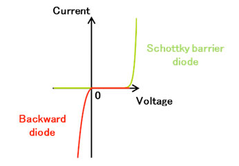 |
| Figure 2. Rectifying Characteristics of a Schottky Barrier Diode and a Backward Diode. Unlike conventional Schottky barrier diodes, backward diodes have steeply-sloped rectifying characteristics with zero bias. |
| This research group succeeded in forming a backward diode1) that possesses excellent rectification characteristics even within low voltage ranges in a nanowire2) that has been miniaturized to a width of about one thousandth the width of a strand of hair. The newly-developed nanowire backward diode achieved a level of sensitivity more than 10 times higher than conventional Schottky barrier diodes.3) |
| With this technology, microwaves with a power level of 100 nanowatts (nW) can be converted to electricity. Going forward, as the research group optimize the design of the diode and the radio wave-collecting antenna while adding power control for constant voltage, there are high expectations for the realization of energy harvesting from environmental radio waves. |
| The results of this research ("Highly Sensitive p-GaAsSb/n-InAs Nanowire Backward Diodes for Low-Power Microwaves") will be announced on September 26, 2019, at the European Solid-State Device Research Conference (ESSDERC), an international conference being held in Krakow, Poland. |
Research Details |
| The researchers carried out development to create a diode with higher sensitivity (figure 2). Specifically, they shrunk the capacity of and miniaturized a backward diode that is capable of steep rectification operations with zero bias4), as rectification occurs by joining two different types of semiconductors and current flows with a different principle (tunnel effect) than conventional Schottky barrier diodes. |
| Conventional backward diodes were formed by processing the thin film of a layered compound semiconductor into a disk shape via etching. Nonetheless, because the materials are prone to damage under processing, it was difficult to finely process diodes to a submicron size and operate them. |
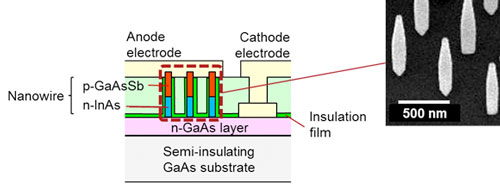 |
| Figure 3. Cross-section of the Nanowire Backward Diode and the Nanowire Crystals. Just by growing crystals, without using an etching process, extremely thin nanowires with a width of about one thousandth that of a strand of hair, were formed on a semiconductor substrate. With this process, electrodes can be formed without infecting damage to the nanowire. |
| By adjusting the ratio (composition) of the constituent elements of the connected semiconductor materials and, at a minute level, the density of the added impurities, the researchers succeeded in growing crystals in nanocrystals with a diameter of 150nm comprised of n-type indium arsenide (n-InAs) and p-type gallium arsenide antimonide (p-GaAsSb) for a tunnel junction structure necessary for the characteristics of the backward diode. |
| Moreover, in the process for implanting insulating material around the nanowire and the process for forming electrode film with metal on both end of the wire, a new technology was used for mounting that does not damage the nanowire. As a result, they were able to form a sub-micron sized diode, which was difficult to do with conventional miniaturization process technology for compound semiconductors, and thereby succeeded, for the first time in the world, in developing a nanowire backward diode with over 10 times the sensitivity of conventional Schottky barrier diodes (figure 3). |
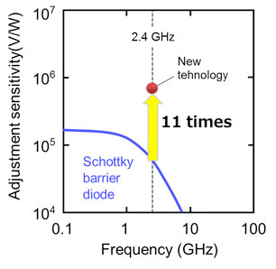 |
| Figure 4. Sensitivity Characteristics of the Diode. In the microwave frequency band of 2.4GHz, which is currently used for 4G LTE and Wi-Fi, a level of sensitivity was achieved that is 11 times that of a conventional Schottky barrier diode. |
| In testing the new technology in the microwave frequency of 2.4GHz, which is currently used in the 4G LTE and Wi-Fi communication line standards for mobile phones, the sensitivity was 700kV/W, roughly 11 times that of the conventional Schottky barrier diode (with a sensitivity of 60KV/W) (figure 4). |
| Therefore, the technology can efficiently convert 100nW-class low-power radio waves into electricity, enabling the conversion of microwaves emitted into the environment from mobile phone base stations in an area that is over 10 times greater than was previously possible (corresponding to 10% of the area in which mobile phone communications are possible). This has led to expectations that it can be used as a source of power for sensors (figure 5). |
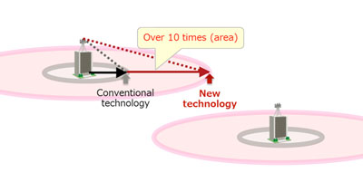 |
| Figure 5. Effect of the Newly-Developed Nanowire Backward Diode |
| By using the newly-developed nanowire backward diode as the rectifying element, electricity can be converted in an area that is over 10 times as large as that achieved using a conventional Schottky barrier diode (corresponding to 10% of the area in which mobile phone communications are possible). |
| In the microwave frequency band of 2.4GHz, which is currently used for 4G LTE and Wi-Fi, a level of sensitivity was achieved that is 11 times that of a conventional Schottky barrier diode. |
Future Plans |
| In the future, it is expected that the newly-developed nanowire backward diode will be applied in using plentiful ambient radio wave energy in 5G communications, serving as a stable power source of sensors and contributing to battery-free sensors used to monitor infrastructure such as constructions and buildings. |
| Going forward, the research group will further increase the sensitivity of the diode, optimize the diode-integrated antenna, and add power control for voltage consistency, aiming to realize a technology that can generate power anywhere using ambient radio waves. |
Notes |
| 1) Backward diode: In contrast to conventional Schottky barrier diodes, these diodes operate by using the phenomenon of tunneling. They enable excellent rectification operations even within small voltage ranges in which conventional diodes are unable to achieve sufficient rectification. |
| 2) Nanowire: Wire-shaped semiconductors so thin that their width is measured in nanometers (nm). Rather than through top-down processing such as etching, they can be built bottom up through crystal formation. |
| 3) Schottky barrier diode: Diodes that use the energy known as a Schottky barrier, which is produced through a junction of a semiconductor and metal, for rectification. |
| 4) Zero bias: A condition in which there is zero voltage. With the harvesting of energy from environmental radio waves, zero bias operations are needed because power cannot be consumed for the adjustment of the operating voltage. |
| Source: Fujitsu |
|
Subscribe to a free copy of one of our daily Nanowerk Newsletter Email Digests with a compilation of all of the day's news. |

