| Oct 14, 2019 |
Scientists reveal mechanism of electron charge exchange in molecules(Nanowerk News) Researchers at the University of California, Irvine have developed a new scanning transmission electron microscopy method that enables visualization of the electric charge density of materials at sub-angstrom resolution. |
| With this technique, the UCI scientists were able to observe electron distribution between atoms and molecules and uncover clues to the origins of ferroelectricity, the capacity of certain crystals to possess spontaneous electric polarization that can be switched by the application of an electric field. |
| The research, which is highlighted in a study published in Nature ("Real-space charge-density imaging with sub-ångstrom resolution by four-dimensional electron microscopy"), also revealed the mechanism of charge transfer between two materials. |
| “This method is an advancement in electron microscopy – from detecting atoms to imaging electrons – that could help us engineer new materials with desired properties and functionalities for devices used in data storage, energy conversion and quantum computing,” said team leader Xiaoqing Pan, UCI’s Henry Samueli Endowed Chair in Engineering and a professor of both materials science & engineering and physics & astronomy. |
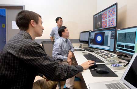 |
| Christopher Addiego (left), a UCI graduate student in physics & astronomy; Xiaoqing Pan (seated in center), UCI’s Henry Samueli Endowed Chair in Engineering and a professor of both materials science & engineering and physics & astronomy; and Wenpei Gao (standing), a UCI postdoctoral researcher in materials science & engineering, were able to visualize the electric charge density of materials at sub-angstrom resolution using a new scanning transmission electron microscopy technique. (Image: Steve Zylius / UCI) |
| Employing a new aberration-corrected scanning transmission electron microscope with a fine electron probe measuring half an angstrom and a fast direct electron detection camera, his group was able to acquire a 2D raster image of diffraction patterns from a region of interest in the sample. As obtained, the data sets are 4D, since they consist of 2D diffraction patterns from each probe location in a 2D scanning area. |
| “With our new microscope, we can routinely form an electron probe as small as 0.6 angstrom, and our high-speed camera with angular resolution can acquire 4D STEM images with 512 x 512 pixels at greater than 300 frames per second,” Pan said. “Using this technique, we can see the electron charge distribution between atoms in two different perovskite oxides, non-polar strontium titanate and ferroelectric bismuth ferrite.” |
| Electron charge density in bulk materials can be measured by X-ray or electron diffraction techniques by assuming a perfectly defect-free structure within the beam-illuminated area. But, Pan said, there remains a challenge in resolving electron charge density in nanostructured materials consisting of interfaces and defects. |
| “In principle, local electric field and charge density can be determined by electron diffraction imaging using an aberration-corrected scanning transmission electron microscope with a sub-angstrom electron probe,” he said. “While penetrating through a specimen, the electron beam interacts with the internal electric field of material in its pathway, resulting in a change in its momentum reflected in the diffraction pattern. By measuring this change, the electric field in a local region of the specimen can be delineated, and the charge density can be derived.” |
| Pan added that although this principle has been demonstrated in simulations, no experiment has been successful until now. |
| “The electron charge density maps obtained using the 4D STEM method match with theoretical results from the first-principle calculations,” said lead author Wenpei Gao, a UCI postdoctoral researcher in materials science & engineering. “The study of the ferroelectric/insulator interface between bismuth ferrite and strontium titanate using this technique directly shows how features of the bismuth compound’s polar atomic structure leak across the interface, appearing in the normally non-polar strontium titanate. As a result, the interface hosts excess electrons confined to a small region less than 1 nanometer thick.” |
| Pan said that this project gives materials scientists and engineers new tools for evaluating structures, defects and interfaces in functional materials and nanodevices. He noted that it may soon be possible to conduct high-throughput mapping of the charge density of materials and molecules to add to the database of properties aiding in the Materials Genome Initiative. |
|
|
| “As electron microscopy advances from imaging atoms to probing electrons, it will lead to new understanding and discovery in materials research,” said co-author Ruqian Wu, UCI professor of physics & astronomy, who led the study’s theoretical work. “The ability to image the charge density distribution around atoms near interfaces, grain boundaries or other planar defects opens new fields for electron microscopy and materials science.” |
| Pan and his team at UCI were joined by collaborators at Cornell University and China’s Nanjing University. The project was supported by the U.S. Department of Energy Office of Basic Energy Sciences’ materials sciences and engineering division, under grant DE-SC0014430. |
| The experiments in the study were carried out using the aberration-corrected scanning transmission electron microscopy facilities in the Irvine Materials Research Institute, of which Pan is the inaugural director. IMRI is a cross-disciplinary organization under UCI’s Office of Research that offers world-class materials characterization facilities to researchers engaged in the discovery, development and commercialization of all types of materials. |
| Source: University of California, Irvine |
|
Subscribe to a free copy of one of our daily Nanowerk Newsletter Email Digests with a compilation of all of the day's news. |

