| Nov 20, 2019 |
The beauty of imperfections: Linking atomic defects to 2D materials' electronic properties(Nanowerk News) Like any material, atomically thin, 2D semiconductors known as TMDs or transition metal dichalcogenides are not perfect, but their imperfections can actually be a good thing. |
| Understanding how defects are structured at the atomic scale, how they are created, and how they interact with electrons are the first steps to designing new advanced materials. However, no one has been able to link useful properties like optical absorption and emission, conductivity, or catalytic function to specific defects in TMDs. |
| Now, two studies led by scientists at the Department of Energy’s Lawrence Berkeley National Laboratory (Berkeley Lab) have revealed surprising details on how some atomic defects emerge in TMDs, and how those defects shape the 2D material’s electronic properties. Their findings could provide a more versatile yet targeted platform for designing 2D materials for quantum information science and smaller, more powerful next-generation light-based electronics (optoelectronics). |
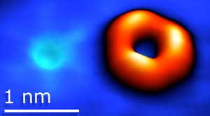 |
| Scanning tunneling microscopy image of an oxygen substituting sulfur (left) and sulfur vacancy (right) in tungsten disulfide. (Image: Berkeley Lab) |
A quantum tip for 2D materials |
| In the world of materials science, many researchers assumed that the most abundant defects in TMDs were the result of missing atoms or “vacancies” of sulfur in tungsten disulfide (WS2), or selenium vacancies in molybdenum diselenide (MoSe2). |
| But as reported in Nature Communications ("Identifying substitutional oxygen as a prolific point defect in monolayer transition metal dichalcogenides"), the researchers found that the defects previously observed with other methods were actually created by oxygen atoms replacing sulfur or selenium atoms, said D. Frank Ogletree, a staff scientist at Berkeley Lab’s Molecular Foundry and a co-author of the two studies. |
| Oxygen, like sulfur and selenium, is part of the oxygen or “chalcogen” family of elements. And since chalcogens share similar properties, there isn’t much change in conductivity when an oxygen atom takes the place of a sulfur or selenium atom in a TMD crystal structure, he said. |
| “In other words, it’s like exchanging one kind of apple for another,” explained co-lead author Bruno Schuler, a postdoctoral researcher at Berkeley Lab’s Molecular Foundry. “So when an oxygen atom fills in for a missing sulfur or selenium atom, it effectively restores the TMD’s electronic properties.” |
| Co-lead author with Schuler is Sara Barja, who was a postdoctoral researcher in Berkeley Lab’s Materials Sciences Division at the time of the Nature Communications study. |
| Key to their finding was the use of the Molecular Foundry’s atomic force microscope (AFM), with a single carbon monoxide (CO) molecule acting as an ultrasharp “tip” or probe, and scanning tunneling microscope (STM). They also benefited from state-of-the-art calculations carried out by scientists from Berkeley Lab’s Center for Computational Study of Excited State Phenomena in Energy Materials (C2SEPEM). |
|
| Atomic force microscopy image of sulfur vacancy in tungsten disulfide. (Image: Berkeley Lab) |
| When used with AFM, the CO-tip images the surface atoms at a very high resolution that’s not possible with conventional techniques, and precisely pinpoints the defect’s atomic site; STM provides the defect’s unique electronic fingerprint. |
| “The combined insights from both of these methods, combined with detailed calculations performed at Berkeley Lab’s National Energy Research Scientific Computing Center (NERSC), ultimately helped us understand what these defects are and why they behave the way they do,” said author Alexander Weber-Bargioni, who led the studies. Weber-Bargioni is the facility director for Imaging and Manipulation of Nanostructures at Berkeley Lab’s Molecular Foundry. |
The unexpected power of an orbiting electron’s spin |
| In the researchers’ second study, published in Physical Review Letters, they demonstrated how to deliberately create chalcogen vacancies by heating a sample of WS2 in vacuum up to 600 degrees Celsius (1,112 degrees Fahrenheit), resulting in a thermal energy that causes the atoms to vibrate. “The vibrations kick out one of the sulfur atoms, creating an atomic hole in the material’s crystalline structure,” explained lead author Schuler. |
| The scientists also discovered that “spin-orbit interaction” – which relates to the properties of electrons orbiting around an atom’s nucleus and in their own inherent directional spin – plays a significant role in the electronic structure of chalcogen vacancies. |
| “In many cases the electron orbital and spin are autonomous and do not care about each other,” he said. “But in some cases, as we discovered in our study, they interact and form hybrid states of electronic structure.” |
| Schuler noted that the impact of spin-orbit interaction on the electronic structure of defect sites in TMDs wasn’t clearly understood before this study. |
|
|
| “It wasn’t even on anyone’s radar. We’re the first to prove it not only by quantitatively determining the magnitude of spin-orbit coupling but also by directly imaging the defect’s electronic orbitals,” he said. |
| Now that the researchers have successfully demonstrated how to create chalcogen vacancies in TMDs, Schuler said that they plan to explore the engineering of atomic defects in other types of 2D materials, such as the creation of distinct spin-polarized states, which would be useful for realizing atomic quantum light emitters and other such devices. |
| Co-corresponding author Jeff Neaton, a senior faculty scientist in Berkeley Lab’s Materials Sciences Division and professor of physics at UC Berkeley, said that Berkeley Lab offers a unique venue for carrying out multidisciplinary studies. |
| “By combining novel experiments at the Molecular Foundry with leading-edge theory, and computing defects’ properties at NERSC with computational methods developed at C2SEPEM, we are steps closer to understanding how common defects can be used to tune optoelectronic properties in 2D materials,” he said. |
| Source: Lawrence Berkeley National Laboratory |
|
Subscribe to a free copy of one of our daily Nanowerk Newsletter Email Digests with a compilation of all of the day's news. |

