| Feb 05, 2020 |
No strain, no gain! breakthrough in 2D material that produces single photons(Nanowerk News) Quantum information technologies need materials that can produce a regular stream of single particles of light (photons). Two-dimensional materials are made of single layers of coordinated atoms. |
| Recent research has shown that these 2D materials may have potential as light sources that emit light as single photons. |
| Scientists discovered a new method to generate single photons (Applied Physics Letters, "Locally defined quantum emission from epitaxial few-layer tungsten diselenide"). They used strain (a system’s response to an applied force) in a 2D material made of tungsten and selenium. By grafting a thin film of the WSe2 onto an ultra-sharp tip made of silicon dioxide, they created specific, well-separated spaces on the thin film that created photons. |
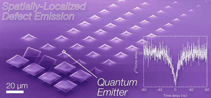 |
| A false-color scanning electron micrograph of the array used to create deterministic single photon sources in epitaxial tungsten diselenide. The inset shows the Hanbury-Brown Twiss interferometry measurement proving quantum emission. (Image: Michael Pettes, Center for Integrated Nanotechnologies, Los Alamos National Laboratory (click on image to enlarge) |
| Generating photons one at a time is essential for quantum communications and certain types of quantum computing. Being able to control thin-film materials so they emit single photons at precise locations will pave the way for scientists to develop quantum materials for use outside of the lab. |
| Previously, scientists didn’t know the mechanism for creating this effect. In addition, it wasn’t possible to produce these materials on a larger scale. The fact that researchers will be able to scale up these 2D tungsten/selenium thin films makes them potentially useful for manufacturing quantum technologies. |
| Scientists discovered a new method for developing sources that emit light as single photons (quantum emitters) by exploiting strain in a two-dimensional material. This method creates spatially localized and well-separated emission sites in a continuous tungsten/selenium thin-film. |
| The film is created by a multi-step diffusion-mediated gas source chemical vapor deposition technique, then transferred onto an array of ultra-sharp silicon dioxide tips. Because the film is very thin, it conforms to the radius of the tips and bends towards the substrate by more than a few percent. |
| The resulting strain is enough to change the electronic structure, but only at the tips. The affected area emits light of a different color and nature than light from the rest of the film. |
| The team observed bound exciton lifetimes that were one order of magnitude longer compared to emissions that were intrinsic to the film. Single photon generation at the tip apex was confirmed by a laser technique called Hanbury-Brown-Twiss quantum interferometry. |
| Future studies looking at the role of mechanical deformation in creating these quantum emission sites may enable a route to control quantum optical properties with strain. While engineering of quantum emission in two-dimensional materials is still at an early stage, this research provides a path toward scale-up to larger quantum material systems. |
| Source: Los Alamos National Laboratory |
|
Subscribe to a free copy of one of our daily Nanowerk Newsletter Email Digests with a compilation of all of the day's news. |

