| Mar 18, 2020 |
Researchers report epitaxial growth of single-crystal hexagonal boron nitride monolayers(Nanowerk News) A research team led by Prof. FU Qiang from the Dalian Institute of Chemical Physics (DICP) of the Chinese Academy of Sciences and their collaborators reported the successful epitaxial growth of single-crystal hexagonal boron nitride (hBN) monolayers on a Cu (111) thin film across a two-inch c-plane sapphire wafer. |
| The results were published in Nature ("Wafer-scale single-crystal hexagonal boron nitride monolayers on Cu (111)"). |
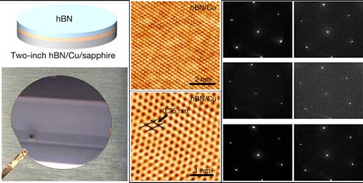 |
| Wafer-scale single-crystal hexagonal boron nitride monolayers identified by STM and micro-region LEED. (Image: LI Rongtan) |
| Ultrathin hexagonal boron nitride is expected to be one of the best candidate materials for future 2D electronics. However, reliable production of wafer-scale single-crystal hBN films which are compatible with advanced microelectronics fabrication processes still remains a challenge. |
| The joint research team first deposited 500 nm thick single-crystal Cu (111) thin films without any twinned grains on c-plane sapphire wafers. Single-crystal hBN monolayers epitaxially grew on the inch-sized substrates. |
| Scientists in DICP used a deep ultraviolet laser photoemission electron microscopy and low-energy electron microscopy (DUV-PEEM/LEEM) system developed by the State Key Lab of Catalysis to characterize the single crystalline quality within the large-area monolayer film. |
| By making use of the unique micro-region surface imaging and surface diffraction capability of the setup, the whole hBN monolayer was revealed to be unidirectionally aligned with the Cu (111) surfaces by probing around one hundred micrometer-sized spots across the one-inch hBN wafer confirming the single-crystallinity of the hBN monolayer films. |
| Source: Chinese Academy of Sciences |
|
Subscribe to a free copy of one of our daily Nanowerk Newsletter Email Digests with a compilation of all of the day's news. |

