| Mar 24, 2020 |
Wrapped, layered semiconductors catch the light(Nanowerk News) Heterostructures are semiconductors made of thin layers of different materials. The combination of materials gives them special optical and electronic properties. This makes them useful in lasers, solar cells, transistors, and other applications. |
| Researchers discovered a new way to integrate semiconductor layers to make heterostructures. They found that layers of different compounds of tin and sulfur spontaneously separated during synthesis. The result is a core of tin sulfide crystals wrapped in a tin disulfide shell. This unique structure translates into excellent light absorption and energy transfer properties (Advanced Materials, "Wrap-Around Core-Shell Heterostructures of Layered Crystals"). |
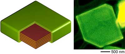 |
| Exposure of tin to sulfur produces a layered, fast-growing tin sulfide core (brown) surrounded by a thin tin disulfide shell (green). An electron microscope that can detect light transmitting particles (photons) revealed intense light from the edges. (Image: Peter Sutter, University of Nebraska-Lincoln) |
| The researchers used a simple and efficient new method to spontaneously form high-quality semiconductor layers with a core-shell structure. The simple process means these new heterostructures could be relatively easy to produce. The structures absorb light using their core, shell, and the interfaces between the components. This translates into enhanced light harvesting. |
| The heterostructures are promising for applications using the sun to accelerate chemical reactions. For example, they could have a role in electricity and fuel production. |
| A good cake often combines different layers to create a combination of flavors and textures. Like a good cake, heterostructures combine different semiconductor materials to do new things. For example, heterostructures can convert absorbed solar energy to make electricity and fuels. |
| The researchers developed a new heterostructure of layered crystal materials that formed spontaneously during one-pot synthesis. One-pot synthesis is a strategy in chemistry that improves efficiency by subjecting a material to successive chemical reactions in the same vessel. Other methods require additional preparation and purification steps. |
| The researchers used this process to expose tin to sulfur. The novel process created a heterostructure in which tin disulfide forms a shell that wraps around layers of tin sulfide. Tin sulfide and tin disulfide consist of the same elements (tin and sulfur), but in different proportions, resulting in different layered crystal structures that produce different semiconductor properties. |
| The researchers then examined the heterostructure under an electron microscope that has a new ability to probe optical properties related to energy transfer, in additional to high-resolution imaging capabilities. They found that the new heterostructure has an unusual capacity to absorb light, including infrared photon energy. |
| Source: U.S. Department of Energy, Office of Science |
|
Subscribe to a free copy of one of our daily Nanowerk Newsletter Email Digests with a compilation of all of the day's news. |

