| Apr 22, 2020 | |
The future of semiconductors is clear(Nanowerk News) Mobility is a key parameter for semiconductor performance and relates to how quickly and easily electrons can move inside a substance. Researchers have achieved the highest mobility among thin films of tin dioxide ever reported (Scientific Reports, "High mobility approaching the intrinsic limit in Ta-doped SnO2 films epitaxially grown on TiO2 (001) substrates"). |
|
| This high mobility could allow engineers to create thin and even transparent tin dioxide semiconductors for use in next-generation LED lights, photovoltaic solar panels or touch-sensitive display technologies. | |
| Tin and oxygen are very familiar elements, and when combined in a certain way to become tin dioxide, the material can be made into a semiconductor. Semiconductors are fundamental to most of our technology and are the basis of computer chips, solar panels and more. | |
 |
|
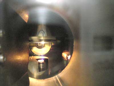
| Laser deposition. A focused laser is used to create thin films of tin dioxide. © Scientific Reports) | |
| Since the 1960s, tin dioxide specifically has found use in industrial applications like gas sensors and transparent electrodes for solar devices. The material is effective for these things because of its high mobility. For most applications, higher is better. However, the high mobility of tin oxide only existed in large bulk crystals, until now. | |
| “We demonstrated the highest mobility in a thin film of tin oxide ever achieved. Improved mobility not only enhances the conductivity but also the transparency of the material,” said Shoichiro Nakao, a researcher from the Department of Chemistry at the University of Tokyo. “Generally, transparency and conductivity cannot coexist in a material. Typical transparent materials such as glass or plastic are insulating, whereas conducting materials like metals are opaque. Few materials exhibit transparent conductivity — it’s very interesting!” | |
 |
|
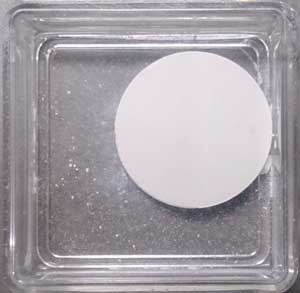
| Tin dioxide pellet. The raw material used to make tin dioxide semiconductors. © Scientific Reports) | |
| The more transparent a semiconductor can be, the more light it can let through. Nakao and his team have made a tin oxide thin film that allows visible light and near-infrared light to pass. This is a great benefit to the power conversion efficiency of photovoltaic solar panels, but other uses could include enhanced touch-screen displays with even better accuracy and responsiveness, or more efficient LED lights. | |
| “Our method of production was key to creating a substance with these properties. We used a highly focused laser to evaporate pellets of pure tin dioxide and deposit or grow material exactly how we wanted it,” said Nakao. “Such a process allows us to explore different growth conditions as well as how to incorporate additional substances. This means we can endow tin dioxide semiconductors with high mobility and useful functionality.” |
| Source: University of Tokyo | |
|
Subscribe to a free copy of one of our daily Nanowerk Newsletter Email Digests with a compilation of all of the day's news. |
