| Aug 06, 2020 |
Scientists zero in on bismuth vanadate's role in renewable energy at the nanoscale(Nanowerk News) In the fight against climate change, scientists have searched for ways to replace fossil fuels with carbon-free alternatives such as hydrogen fuel. |
| A device known as a photoelectrical chemical cell (PEC) has the potential to produce hydrogen fuel through artificial photosynthesis, an emerging renewable energy technology that uses energy from sunlight to drive chemical reactions such as splitting water into hydrogen and oxygen. |
| The key to a PEC’s success lies not only in how well its photoelectrode reacts with light to produce hydrogen, but also oxygen. Few materials can do this well, and according to theory, an inorganic material called bismuth vanadate (BiVO4) is a good candidate. |
| Yet this technology is still young, and researchers in the field have struggled to make a BiVO4 photoelectrode that lives up to its potential in a PEC device. |
| Now, as reported in the journal Small ("Revealing Nanoscale Chemical Heterogeneities in Polycrystalline Mo-BiVO4 Thin Films"), a research team led by scientists at the Department of Energy’s Lawrence Berkeley National Laboratory (Berkeley Lab) and the Joint Center for Artificial Photosynthesis (JCAP), a DOE Energy Innovation Hub, have gained important new insight into what might be happening at the nanoscale (billionths of a meter) to hold BiVO4 back. |
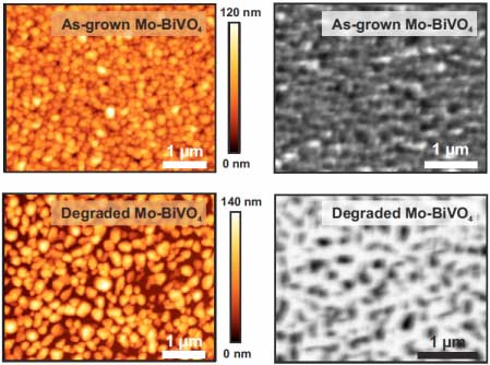 |
| Left: Atomic force microscopy images of Mo-BiVO4 thin films before degradation (top-left) and after degradation (bottom-left); corrosion causes the grains of the material to disconnect from each other. Right: X-ray absorption maps of Mo-BiVO4 thin films before degradation (top-right) and after degradation (bottom-right); the dark areas correspond to areas with high concentration of Mo-BiVO4, whereas the bright areas indicate regions with low concentration of Mo-BiVO4. (Image: Berkeley Lab) |
| “When you make a material, such as an inorganic material like bismuth vanadate, you might assume, just by looking at it with the naked eye, that the material is homogeneous and uniform throughout,” said senior author Francesca Toma, a staff scientist at JCAP in Berkeley Lab’s Chemical Sciences Division. “But when you can see details in a material at the nanoscale, suddenly what you assumed was homogeneous is actually heterogeneous – with an ensemble of different properties and chemical compositions. And if you want to improve a photoelectrode material’s efficiency, you need to know more about what’s happening at the nanoscale.” |
X-rays and simulations bring a clearer picture into focus |
| In a previous study (Nature Communications, "Nanoscale imaging of charge carrier transport in water splitting photoanodes") supported by the Laboratory Directed Research and Development program, Toma and lead author Johanna Eichhorn developed a special technique using an atomic force microscope at Berkeley Lab’s JCAP laboratory to capture images of thin-film bismuth vanadate at the nanoscale to understand how a material’s properties can affect its performance in an artificial photosynthesis device. (Eichhorn, who is currently at the Walter Schottky Institute of the Technical University of Munich in Germany was a researcher in Berkeley Lab’s Chemical Sciences Division at the time of the study.) |
| The current study builds on that pioneering work by using a scanning transmission X-ray microscope (STXM) at Berkeley Lab’s Advanced Light Source (ALS), a synchrotron user facility, to map out changes in a thin-film semiconducting material made of molybdenum bismuth vanadate (Mo-BiVO4). |
| The researchers used bismuth vanadate as a case example of a photoelectrode because the material can absorb light in the visible range in the solar spectrum, and when combined with a catalyst, its physical properties allow it to make oxygen in the water-splitting reaction. Bismuth vanadate is one of the few materials that can do this, and in this case, the addition of a small quantity of molybdenum to BiVO4 somehow improves its performance, Toma explained. |
| When water is split into H2 and O2, hydrogen-hydrogen and oxygen-oxygen bonds need to form. But if any step in water-splitting is out of sync, unwanted reactions will happen, which could lead to corrosion. “And if you want to scale up a material into a commercial water-splitting device, no one wants something that degrades. So we wanted to develop a technique that maps out which regions at the nanoscale are the best at making oxygen,” Toma explained. |
| Working with ALS staff scientist David Shapiro, Toma and her team used STXM to take high-resolution nanoscale measurements of grains in a thin film of Mo-BiVO4 as the material degraded in response to the water-splitting reaction triggered by light and the electrolyte. |
| “Chemical heterogeneity at the nanoscale in a material can often lead to interesting and useful properties, and few microscopy techniques can probe the molecular structure of a material at this scale,” Shapiro said. “The STXM instruments at the Advanced Light Source are very sensitive probes that can nondestructively quantify this heterogeneity at high spatial resolution and can therefore provide a deeper understanding of these properties.” |
| David Prendergast, interim division director of the Molecular Foundry, and Sebastian Reyes-Lillo, a former postdoctoral researcher at the Foundry, helped the team understand how Mo-BiVO4 responds to light by developing computational tools to analyze each molecule’s spectral “fingerprint.” Reyes-Lillo is currently a professor at Andres Bello University in Chile and a Molecular Foundry user. The Molecular Foundry is a Nanoscale Science Research Center national user facility. |
| “Prendergast’s technique is really powerful,” Toma said. “Often when you have complex heterogeneous materials made of different atoms, the experimental data you get is not easy to understand. This approach tells you how to interpret those data. And if we have a better understanding of the data, we can create better strategies for making Mo-BiVO4 photoelectrodes less vulnerable to corrosion during water-splitting.” |
| Reyes-Lillo added that Toma’s use of this technique and the work at JCAP enabled a deeper understanding of Mo-BiVO4 that would otherwise not be possible. “The approach reveals element-specific chemical fingerprints of a material’s local electronic structure, making it especially suited for the study of phenomena at the nanoscale. Our study represents a step toward improving the performance of semiconducting BiVO4-based materials for solar fuel technologies,” he said. |
Next steps |
| The researchers next plan to further develop the technique by taking STXM images while the material is operating so that they can understand how the material changes chemically as a photoelectrode in a model PEC system. |
| “I’m very proud of this work. We need to find alternative solutions to fossil fuels, and we need renewable alternatives. Even if this technology isn’t ready for the marketplace tomorrow, our technique – along with the powerful instruments available to users at the Advanced Light Source and the Molecular Foundry – will open up new routes for renewable energy technologies to make a difference.” |
| Source: Lawrence Berkeley National Laboratory |
|
Subscribe to a free copy of one of our daily Nanowerk Newsletter Email Digests with a compilation of all of the day's news. |

