| Nov 20, 2020 |
More Moore: Development of ultra-thin semiconductor electrodes
(Nanowerk News) Since the Moore’s law, which states that the density of semiconductor integrated circuits one can most economically manufacture doubles approximately every 2 years, is broken, research is actively being conducted to investigate new and promising semiconductor materials.
|
|
More Moore refers to an attempt to develop a smaller, better-performing semiconductor out of materials other than silicon.
|
|
A research team, led by Professor Soon-Yong Kwon in the School of Materials Science and Engineering at UNIST has succeeded in patterning the two-dimensional (2D) metal electrode, which has long been identified as an obstacle to the realization of high-performance ultra-fine semiconductors, into desired shapes on the 4-inch diameter silicon substrate (Nature Electronics, "Wafer-scale production of patterned transition metal ditelluride layers for two-dimensional metal–semiconductor contacts at the Schottky–Mott limit").
|
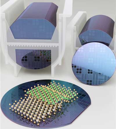 |
| Figure 1. Schematic image showing the wafer-scale production of patterned layers of metallic transition metal ditellurides on large-scale substrates. (Image: Professor Soon-Yong Kwon, UNIST)
|
|
In order to improve the performance of semiconductor chips, the individual elements constituting the chip must be made very small. There are drawbacks, however, in the challenge of miniaturization and integration of the existing silicon-based electron devices. Because of this, the development of More Moore semiconductors using thin materials, such as graphene is crucial.
|
|
The new 2D metal electrode is only one atom thick, and thus can be applied to thin film materials for the semiconductor devices, such as graphene. This is expected to accelerate the miniaturization of semiconductor devices, according to the research team.
|
|
Semiconductor devices works properly only when the electrons flow in a particular position and direction that they desire. However, if you make individual elements too small because you wish to add more elements on a single semiconductor chip, electrons start to flow undesirably (Tunneling Effect).
|
|
To address this challenge, there has been much discussion recently about the use of ultrathin 2D semiconductor materials, yet the electrode suitable for this has not been developed.
|
|
Semiconductors have properties in between those of normal conductors, like metals, and insulators. Therefore, if only the semiconductor material is changed, a relatively high potential barrier (i.e. Schottky barrier) is formed and this makes electron transport difficult. And thus, for the realization of high-performance ultrathin semiconductor devices, 2D electrode materials must be newly synthesized, as well.
|
|
In the study, the research team reported the wafer-scale production of patterned layers of metallic transition metal ditellurides on different substrates. According to the research team, “Our tungsten ditelluride and molybdenum ditelluride layers, which are grown using a tellurization process applied to a precursor transition metal layer, have an electronic performance comparable to that of mechanically exfoliated flakes and can be combined with the 2D semiconductor molybdenum disulfide.”
|
|
“It has been confirmed that the addition of an appropriate amount of tellurium to a specific metal, such as copper (Cu) or nickel (Ni), it becomes liquefied even at a relatively low temperature,” says Seunguk Song in the Doctoral Program of Mechanical Engineering at UNIST, the first author of the research.
|
|
According to the research team, the resulting metal–semiconductor junctions are free from significant disorder effects and Fermi-level pinning (FLP), and their SBHs largely follow the Schottky–Mott limit. The newly synthesized 2D electrode material showed few physical defects during synthesis, and thus exhibited excellent physical and electrical properties that were comparable to mechanically separated 2D materials.
|
|
In addition, the entire process is performed in a few minutes at temperatures less than 500 °C. It also lowers operating costs, as it can be implemented in the existing semiconductor processing.
|
|
The research team also conducted an experiment of placing the 2D semiconductor molybdenum disulfide (MoS2) on a new 2D electrode. As a result, the Schottky barrier between the deposited metal electrode and 2D semiconductor interface was relatively low, similar to the theoretical value, and thus providing a superior path for electron transport.
|
|
“Our technique provides a simple and efficient method to grow high-quality, stoichiometric transition metal ditellurides with an electrical performance comparable to that of mechanically exfoliated flakes,” the authors noted.
|
|
“The fabricated 2D vdW interfaces are free from substantial disorder effects and FLP, and their SBHs largely follow the Schottky–Mott limit,” says Professor Kwon.
|

