| Mar 25, 2021 |
Exploring the nanoworld in 3D
(Nanowerk News) Imagine a cube on which light is projected by a flashlight. The cube reflects the light in a particular way, so simply spinning the cube or moving the flashlight makes it possible to examine each aspect and deduce information regarding its structure. Now, imagine that this cube is just a few atoms high, that the light is detectable only in infrared, and that the flashlight is a beam from a microscope.
|
|
How to go about examining each of the cube's sides? That is the question recently answered by scientists from the CNRS, l'Université Paris-Saclay, the University of Graz and Graz University of Technology (Austria) by generating the first 3D image of the structure of the infrared light near the nanocube.
|
|
Their results are published in Science ("Three-dimensional vectorial imaging of surface phonon polaritons").
|
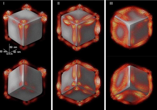 |
| 3D reconstruction of the electromagnetic field surrounding a magnesium oxide nanocube. The three modes (I, II, III) represent the nanocube's different energy absorptions. (Image: G. Habelferner, University of Graz)
|
|
Electron microscopy uses an electron beam to illuminate a sample and create an enlarged image. It also provides more complete measurements of physical properties, with unrivalled spatial resolution that can even visualize individual atoms. Chromatem, the Equipex Tempos team's dedicated instrument for spectroscopy1, is one of these new generation microscopes. It probes the optical, mechanical, and magnetic properties of matter with very high resolution, one that is matched by only three other microscopes in the world.
|
|
Scientists from the CNRS and l'Université Paris-Saclay working at the Solid States Physics Laboratory (CNRS/Université Paris-Saclay), along with their colleagues at the University of Graz and Graz University of Technology (Austria), used Chromatem to study a magnesium oxide nanocrystal. The vibration of its atoms creates an electromagnetic field that can only be detected in the mid-infrared range2.
|
|
When the electrons emitted by the microscope indirectly encounter this electromagnetic field, they lose energy. By measuring this energy loss, it becomes possible to deduce the outlines of the electromagnetic field surrounding the crystal. The problem is that this type of microscopy can only provide images in 2D, raising the question of how to visualize all of the cube's corners, edges, and sides.
|
|
In order to do so, the scientists developed image reconstruction techniques that have, for the first time, generated 3D images of the field surrounding the crystal. This will eventually enable targeting a specific point on the crystal, and conducting localized heat transfers, for instance.
|
|
Many other nano-objects absorb infrared light, such as during heat transfers, and it will now be possible to provide 3D images of these transfers. This is one avenue of exploration for optimizing heat dissipation in the increasingly small components used in nanoelectronics.
|
Notes
|
|
1 Tempos is an electron microscopy platform led by l'Université Paris-Saclay, the CNRS, l'École polytechnique, and the CEA. Chromatem, one of its three microscopes, is a unique spectrometer. Spectrometry can decompose a light beam into its constituent elements, which make up its spectrum. It can analyse a wide range of wavelengths, including infrared.
|
|
2 Infrared radiation has a longer wavelength than that of the visible spectrum. Mid-infrared refers to wavelengths between 2 and 20 micrometres. The analysis of infrared radiation is especially used to study heat transfer in materials, as well as for thermal imaging.
|

