| Apr 01, 2021 |
2D materials combine, becoming polarized and giving rise to photovoltaic effect
(Nanowerk News) For the first time, researchers have discovered a way to obtain polarity and photovoltaic behavior from certain nonphotovoltaic, atomically flat (2D) materials.
|
|
The key lies in the special way in which the materials are arranged. The resulting effect is different from, and potentially superior to, the photovoltaic effect commonly found in solar cells.
|
|
Solar power is considered a key technology in the move away from fossil fuels. Researchers continually innovate more efficient means to generate solar energy. And many of these innovations come from the world of materials research.
|
|
Research Associate Toshiya Ideue from the University of Tokyo’s Department of Applied Physics and his team are interested in the photovoltaic properties of 2D materials and their interfaces where these materials meet (Science, "A van der Waals interface creating in-plane polarization and a spontaneous photovoltaic effect").
|
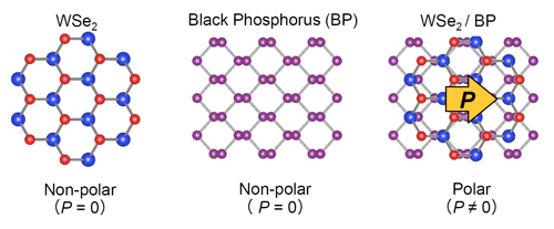 |
| 2D materials. Tungsten selenide (WSe2) and black phosphorus (BP) do not exhibit polarized electronic behavior until combined such that their structures overlap. (© Science)
|
|
“Quite often, interfaces of multiple 2D materials exhibit different properties to the individual crystals alone,” said Ideue. “We have discovered that two specific materials which ordinarily exhibit no photovoltaic effect do so when stacked in a very particular way.”
|
|
The two materials are tungsten selenide (WSe2) and black phosphorus (BP), both of which have different crystal structures. Originally, both materials are nonpolar (do not have a preferred direction of conduction) and do not generate a photocurrent under light.
|
|
However, Ideue and his team found that by stacking sheets of WSe2 and BP together in the right way, the sample exhibited polarization, and when a light was cast on the material, it generated a current. The effect takes place even if the area of illumination is far from the electrodes at either end of the sample; this is different from how the ordinary photovoltaic effect works.
|
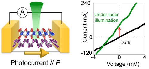 |
| Photovoltaic effect. Under laser illumination, the layered material generates a current. (© Science)
|
|
Key to this behavior is the way the WSe2 and BP are aligned. The crystalline structure of BP has reflective, or mirror, symmetry in one plane, whereas WSe2 has three lines of mirror symmetry. When the symmetry lines of the materials align, the sample gains polarity.
|
|
This kind of layer stacking is delicate work, but it also reveals to researchers new properties and functions that could not be predicted just by looking at the ordinary form of the materials.
|
|
“The biggest challenge for us will be to find a good combination of 2D materials with higher electric-generation efficiency and also to study the effect of changing the angles of the stacks,” said Ideue. “But it’s so rewarding to discover never-before-seen emergent properties of materials. Hopefully, one day this research could improve solar panels. We would like to explore more unprecedented properties and functionalities in nanomaterials.”
|

