| May 07, 2021 |
Discovery of huge Raman scattering at atomic point contact
(Nanowerk News) Nanofabrication of electronic devices has reached a single nanometer scale. The rapid advancement of nanoscience and nanotechnology now requires atomic-scale optical spectroscopy in order to characterize atomistic structures that will affect the properties and functions of the electronic devices.
|
|
The research team further demonstrated tha
The international team headed by Takashi Kumagai at Institute for Molecular Science discovered a huge enhancement of Raman scattering mediated by a formation of an atomic point contact between a plasmonic silver tip and a Si(111)-7×7 reconstructed surface. This was achieved by means of state-of-the-art low-temperature tip-enhanced Raman spectroscopy which allows to conduct atomic-scale vibrational spectroscopy (Nano Letters, "Atomic Point Contact Raman Spectroscopy of a Si(111)-7 × 7 Surface").
|
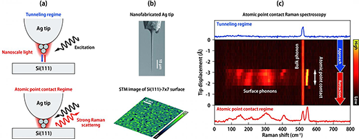 |
| Figure 1. (a) Illustration of the experiment. (b) Scanning electron micrograph of a Ag tip (top) and scanning tunneling microscopy image of the Si(111)-7×7 surface. (c) Atomic point contact Raman spectra. (Image: NINS/IMS) (click on image to enlarge)
|
|
The discovered enhancement mechanism of Raman scattering will open the possibility of atomic-scale ultrasensitive vibrational spectroscopy to investigate surface structures of semiconductors. In addition, the developed atomic-scale optical microscopy will pave the way for exploring atomic-scale light-matter interactions, leading to a new discipline in light science and technology.
|
|
The research team further demonstrated tha
Super integration of electronic devices has entered a single nanometer scale, calling for analytical methods that can investigate atomic-scale structures and defects in detail. The advancement of scanning near-field optical microscopy has allowed nanoscale imaging and chemical analyses at the nanoscale.
|
|
The research team further demonstrated tha
More recently, the spatial resolution of this technique was demonstrated to reach the atomic scale. In particular, tip-enhanced Raman spectroscopy has drawn increasing attention as ultrasensitive chemical microscopy. However, in order to obtain a Raman signal from semiconductor surfaces, it was necessary to further enhance the sensitivity.
|
|
The research team further demonstrated tha
The research team applied state-of-the-art low-temperature tip-enhanced Raman spectroscopy, developed in collaboration with Fritz-Haber Institute, to obtain the vibration spectra from a silicon surface. Tip-enhanced Raman spectroscopy employs a strong light-matter interaction between a material and nanoscale light (localized surface plasmon resonance) generated at an atomically sharp metallic tip.
|
|
The research team further demonstrated tha
The research team discovered that an atomic point contact formation of a silver tip and a reconstructed Si(111)-7×7 surface leads to a huge enhancement of Raman scattering. Figure 1a illustrates the experiment. A sharp silver tip fabricated by focused ion beam (figure 1b, top) is moved toward the silicon surface (figure 1b, bottom), while monitoring the Raman spectra from the junction. Figure 1c displays the waterfall plot of the obtained Raman spectra, where the horizontal axis the Raman shift, and the color scale the Raman intensity.
|
|
The research team further demonstrated tha
When the tip is in the tunneling regime, only the optical phonon mode of the bulk silicon is observed at 520 cm-1. However, when the atomic point contact between the tip and the surface, the strong Raman scattering from the surface phonon modes suddenly appears. These modes disappear again when the tip is moved away from the surface and the atomic point contact is broken.
|
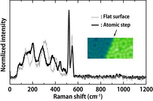 |
| Figure 2. Atomic point contact Raman spectra obtained at an atomic step and a flat surface of the Si(111)-7×7 surface. (Image: NINS/IMS)
|
|
The research team further demonstrated that this atomic point contact Raman spectroscopy (APCRS) can resolve the atomic-scale structures of the silicon surface. As shown in figure 2, the Raman spectrum is different when it is recorded at an atomic step of the surface.
|
|
The research team further demonstrated tha
Furthermore, the characteristic vibration modes can be observed selectively at the locally oxidized site (figure 3), indicating the atomic-scale chemical sensitivity of atomic-point-contact Raman spectroscopy.
|
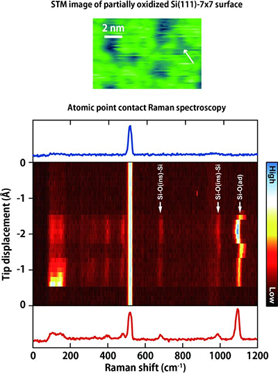 |
| Figure 3. Atomic point contact Raman spectra obtained at a partially oxidized area over the Si(111)-7×7 surface (indicated by the arrow in the STM image). (Image: NINS/IMS)
|
|
It was previously thought that a plasmonic nanogap is necessary to obtain the ultrahigh sensitivity in tip-enhanced Raman spectroscopy, which typically requires a metal substrate. This imposed a severe limitation on measurable samples. The discovery of the huge Raman enhancement upon the atomic point contact formation will expand the potential of atomic-scale vibration spectroscopy, which is applicable to non-plasmonic samples and the exceptional chemical sensitivity will be obtained for many other materials. In addition, these results also suggest that atomic scale structures play an indispensable role in metal-semiconductor hybrid nanosystems to affect their optoelectronic properties.
|


