| Aug 05, 2021 |
A universal intercalation strategy for highly stable perovskite photovoltaics(Nanowerk News) A team of scientists led by the Nanomaterials Research Institute at Kanazawa University have demonstrated that the stability and efficiency of certain solar panels can be greatly enhanced by using cesium iodide (CsI) intercalation technology. |
| This work (Nano Energy, "Double-layer CsI intercalation into an MAPbI3 framework for efficient and stable perovskite solar cells") may help make perovskite solar cells more competitive with other renewable energy sources. |
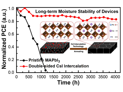 |
| Normalized PCE versus time for unencapsulated PSCs stored in the dark under ambient air without a UV filter at the 40–50% RH. Inset diagram shows the change in crystal structure after CsI intercalation. (Image: Kanazawa University) |
| Solar panels have the potential to be an abundant and clean source of energy. In particular, photovoltaic cells with the perovskite crystal structure, named after the mineral with the same atomic configuration, have many attractive features. Their strong optical absorption and high charge mobilities lead to low cost of manufacture and high energy output. |
| However, deployment by consumers of perovskite solar cells has been hampered by the limited robustness of these cells, because their structure can decompose after exposure to moisture, light, or heat. New formulations that increase the lifetime of perovskite solar cells are thus needed to instill consumer confidence before people start installing perovskite-based solar panels on their roofs. |
| Now, a team of scientists headed by Kanazawa University has discovered that adding CsI to the commonly used MAPbI3 perovskite structure greatly increases the stability of the resulting devices. The Cs atoms migrate and become “intercalated” into the crystal lattice, and the improved devices showed power conversion efficiencies as high as 18.43%. |
| “Hybrid organic-inorganic metal halide perovskite solar cells are a very fast-growing technology,” corresponding author Md. Shahiduzzaman says. |
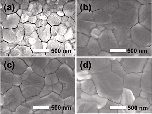 |
| Top view SEM images of a) a pristine MAPbI3 film, and perovskite films with b) up layer, c) down layer and d) double layer CsI intercalation. (Image: Kanazawa University) |
| Using scanning electron microscopy, the scientists verified that the size of the crystal grains inside the material also increased from 300 to 700 nm due to the addition of CsI. They hypothesize that the intercalation of cesium reduces the spacing between the atomic planes, so that moisture from the air cannot intrude as easily. Also, the surfaces become smoother, which allows charges to reach the electrodes. |
| “Our approach allowed us to produce layers with precise control over the CsI intercalation,” corresponding author Tetsuya Taima says. |
| Source: Kanazawa University |

