| Dec 15, 2021 |
Magnetic tunnel junction technology for the Angstrom semiconductor era(Nanowerk News) A research group at Tohoku University has shown that fast switching down to 3.5 ns in sub-five-nm ultra-small magnetic tunnel junctions (MTJs) can be achieved by engineering relaxation time, which governs fast magnetization dynamics (IEEE International Electron Devices Meeting, "Fast Switching Down to 3.5 ns in Sub-5-nm Magnetic Tunnel Junctions Achieved by Engineering Relaxation Time"). |
| The established technology allows for the replacement of SRAM and high-speed DRAM with spintronic non-volatile memory - STT-MRAM - even at the future's Angstrom process nodes. |
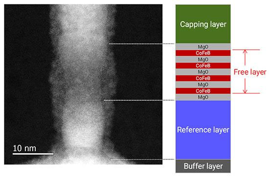 |
| Transmission electron microscope image and film stack of the developed MTJ with the multilayered ferromagnetic structure. Interfacial anisotropy is enhanced by increasing the number of CoFeB/MgO layers. (Image: Butsurin Jinnai and Shunsuke Fukami) |
| STT-MRAM has been intensively developed for the drastic reduction in power consumption of semiconductor integrated circuits (ICs). The required performance for data writing/retention determined by MTJs - a core building block of STT-MRAM - is varied depending on applications. |
| An example of this is long data retention capability (more than 10 years) and is important for flash memory replacement and fast data writing capability (beyond 10 ns) for SRAM replacement. Moreover, the MTJ scaling is always necessary, as is also the case with general semiconductor devices. |
| In 2018, the research group achieved the long data retention performance required for flash memory replacement by shape-anisotropy MTJs at the ultra-small (sub-ten-nm) scale. However, data writing beyond 10 ns has remained a challenge in the shape-anisotropy MTJs. |
| To address it, the research group developed a new multilayered ferromagnetic structure that can engineer characteristic relaxation time, which governs the magnetization dynamics in the ns regime. The MTJs with the multilayered ferromagnetic structure were successfully fabricated down to 2.0 nm, or 20 Angstrom, in diameter (the world's smallest size), and fast switching beyond 10 ns was achieved in sub-five-nm MTJs. |
| "As the newly developed MTJs and the previously developed shape-anisotropy MTJs are complementary to each other in terms of performance, the use of them allows one to fulfill different requirements and needs for a wide variety of applications from the automobile industry and space to IoT and AI in the Angstrom era," said Butsurin Jinnai, the primary author of the study. |
| Principal investigator, Shunsuke Fukami, explained that "our work is expected to contribute to digital-transformation and a carbon-neutral society by speeding up the implementation of STT-MRAM-based semiconductor ICs at future advanced nodes." |
| Source: Tohoku University |

