| May 10, 2022 |
Self-driving microscopes discover shortcuts to new materials
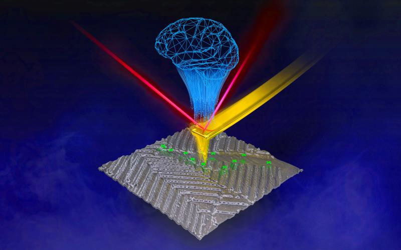
(Nanowerk News) Researchers at the Department of Energy’s Oak Ridge National Laboratory are teaching microscopes to drive discoveries with an intuitive algorithm, developed at the lab’s Center for Nanophase Materials Sciences, that could guide breakthroughs in new materials for energy technologies, sensing and computing.
|
|
“There are so many potential materials, some of which we cannot study at all with conventional tools, that need more efficient and systematic approaches to design and synthesize,” said Maxim Ziatdinov of ORNL’s Computational Sciences and Engineering Division and the CNMS. “We can use smart automation to access unexplored materials as well as create a shareable, reproducible path to discoveries that have not previously been possible.”
|
|
The approach, published in Nature Machine Intelligence ("Experimental discovery of structure–property relationships in ferroelectric materials via active learning"), combines physics and machine learning to automate microscopy experiments designed to study materials’ functional properties at the nanoscale.
|
 |
| A smart approach to microscopy and imaging developed at Oak Ridge National Laboratory could drive discoveries in materials for future technologies. (Image: Adam Malin/ORNL)
|
|
Functional materials are responsive to stimuli such as heat or electricity and are engineered to support both everyday and emerging technologies, ranging from computers and solar cells to artificial muscles and shape-memory materials. Their unique properties are tied to atomic structures and microstructures that can be observed with advanced microscopy. However, the challenge has been to develop efficient ways to locate regions of interest where these properties emerge and can be investigated.
|
|
Scanning probe microscopy is an essential tool for exploring the structure–property relationships in functional materials. Instruments scan the surface of materials with an atomically sharp probe to map out the structure at the nanometer scale — the length of one billionth of a meter. They can also detect responses to a range of stimuli, providing insights into fundamental mechanisms of polarization switching, electrochemical reactivity, plastic deformation or quantum phenomena.
|
|
Today’s microscopes can perform a point-by-point scan of a nanometer square grid, but the process can be painstakingly slow, with measurements collected over days for a single material.
|
|
“The interesting physical phenomena are often only manifested in a small number of spatial locations and tied to specific but unknown structural elements. While we typically have an idea of what will be the characteristic features of physical phenomena we aim to discover, pinpointing these regions of interest efficiently is a major bottleneck,” said former ORNL CNMS scientist and lead author Sergei Kalinin, now at the University of Tennessee, Knoxville. “Our goal is to teach microscopes to seek regions with interesting physics actively and in a manner much more efficient than performing a grid search.”
|
|
Scientists have turned to machine learning and artificial intelligence to overcome this challenge, but conventional algorithms require large, human-coded datasets and may not save time in the end.
|
|
For a smarter approach to automation, the ORNL workflow incorporates human-based physical reasoning into machine learning methods and uses very small datasets — images acquired from less than 1% of the sample — as a starting point. The algorithm selects points of interest based on what it learns within the experiment and on knowledge from outside the experiment.
|
|
As a proof of concept, a workflow was demonstrated using scanning probe microscopy and applied to well-studied ferroelectric materials. Ferroelectrics are functional materials with a reorientable surface charge that can be leveraged for computing, actuation and sensing applications. Scientists are interested in understanding the link between the amount of energy or information these materials can store and the local domain structure governing this property. The automated experiment discovered the specific topological defects for which these parameters are optimized.
|
|
“The takeaway is that the workflow was applied to material systems familiar to the research community and made a fundamental finding, something not previously known, very quickly — in this case, within a few hours,” Ziatdinov said.
|
|
Results were faster — by orders of magnitude — than conventional workflows and represent a new direction in smart automation.
|
|
“We wanted to move away from training computers exclusively on data from previous experiments and instead teach computers how to think like researchers and learn on the fly,” said Ziatdinov. “Our approach is inspired by human intuition and recognizes that many material discoveries have been made through the trial and error of researchers who rely on their expertise and experience to guess where to look.”
|
|
ORNL’s Yongtao Liu was responsible for the technical challenge of getting the algorithm to run on an operational microscope at the CNMS. “This is not an off-the-shelf capability, and a lot of work goes into connecting the hardware and software,” said Liu. “We focused on scanning probe microscopy, but the setup can be applied to other experimental imaging and spectroscopy approaches accessible to the broader user community.”
|

