| May 13, 2022 |
On-chip photodetection: Two-dimensional material heterojunctions hetero-integration
(Nanowerk News) Photonic integrated circuits (PICs) use photons as information carriers and are expected to solve the bottleneck problems of microelectronic chips in terms of speed, power consumption and integration density with their advantages of ultra-high transmission speed, low delay, and anti-electromagnetic crosstalk. It is of key significance to promoting breakthroughs in microelectronics technology, quantum information technology, and micro-sensing technology in the "post-Moore era".
|
|
Currently, driven by the application of information technology, photonic integrated chips (PICs) have made great progress. For example, silicon PIC is compatible with the mature CMOS technology for low-cost and large-scale production; Silicon nitride PIC could tolerate moderately high optical power and large fabrication errors; Lithium niobate PIC could achieve perfect electro-optic modulations with low driven voltage and high linearity.
|
|
However, one of the handicaps in these PICs is the monolithic integration of waveguides and photodetectors with a single material. To support the light transmission in the waveguide, the PIC materials cannot absorb the optical signal, making it impossible to realize the integrated photodetector out of a single material.
|
|
To solve this, hetero-integrations of absorptive bulk materials (such as Ge, III-V compound semiconductors, etc.) on PICs have been implemented. It though still present open challenges such as the high costs, complicated fabrication processes and material interface issues.
|
|
Recently, two-dimensional (2D) materials have emerged as an attractive photon-absorption material for chip-integrated photodetectors. 2D materials have no surface dangling bonds, which eliminates the lattice-mismatch constraints to hetero-integrate them with PICs.
|
|
The family of 2D materials has a rich variety of electronic and optical properties, including semi-metallic graphene, insulating boron nitride, semiconducting transition metal dichalcogenides and black phosphorus. As a consequence, chip-integrated photodetectors operating at various spectral ranges could be constructed by choosing appropriate 2D materials.
|
|
In a new paper published in Light Science & Application ("Chip-integrated van der Waals PN heterojunction photodetector with low dark current and high responsivity"), a research group, led by Professor Xuetao Gan from Key Laboratory of Light Field Manipulation and Information Acquisition, Ministry of Industry and Information Technology, and Shaanxi Key Laboratory of Optical Information Technology, School of Physical Science and Technology, Northwestern Polytechnical University, China have reported that integrating van der Waals PN heterojunctions of 2D materials on optical waveguides can provide a promising strategy to realize chip-integrated photodetectors with low dark current, high responsivity, and fast speed.
|
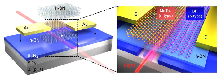 |
| Figure 1. Schematic of the waveguide-integrated van der Waals PN heterojunction photodetector. (Image courtesy of the researchers)
|
|
With the 2D layered structure and no dangling bonds, researchers can stack 2D materials with different properties in different orders by "stacking wood" to form van der Waals heterostructures with atomically flat interfaces.
|
|
The "arbitrary combination" of van der Waals heterojunctions can not only give the advantages properties of a single material, but also generate novel properties, achieving a leap of 1+1>2, as shown in Figure 1.
|
|
In this research, the researchers made full use of natural p-doped BP and n-doped MoTe2 for hetero-stacking, and successfully fabricated an efficient van der Waals PN heterojunction.
|
|
Second, since there are no dangling bonds on the surface of 2D materials, compared with traditional semiconductors, 2D materials do not need to consider lattice mismatch when integrating with various photonic integration platforms.
|
|
Finally, the preparation of source-drain electrodes can also be integrated on the photonic platform through the "stacking wood" technology and placed on both sides of the material, without the cumbersome processes such as photolithography.
|
|
This also greatly simplifies the fabrication process of the device and reduces the fabrication cost of the device. This also greatly simplifies the fabrication process of the device, avoiding the contamination of the device interface in processes such as photolithography, which greatly improves the performance of the device.
|

