| Sep 15, 2022 |
Size matters in functional materials
(Nanowerk News) A collaboration lead by DESY scientists has found a surprising behaviour of the quantum material vanadium dioxide (VO2) at the high-brilliance X-ray source PETRA III. Vanadium dioxide switches from an insulator into a conductive metal at a very common temperature of approximately 70 °C and is therefore very much in the focus of researchers as a possible functional material.
|
|
Together with colleagues from Kiel University, the Helmholtz-Zentrum Berlin as well as from the Paul-Scherrer Institute in Switzerland, the scientists used an X-ray spectro-microscope to study thin-film structures of vanadium dioxide in detail.
|
|
The study (Scientific Reports, "Microstructure effects on the phase transition behavior of a prototypical quantum material") revealed that the transition temperature when the material becomes conducting is not exactly the same across microsquares with a size of 30 by 30 microns: The edges proceed through the transition at temperatures which are lower by 1.2 °C in comparison to the centres.
|
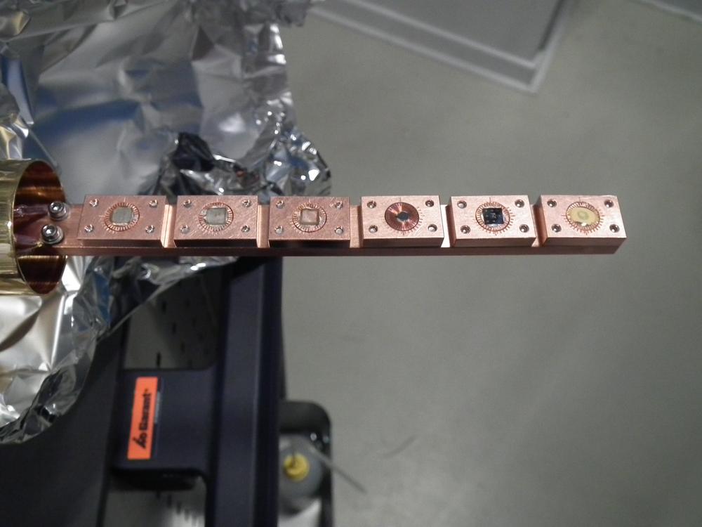 |
| The samples with the tiny vanadium dioxide squares are mounted on this holder. (Image: DESY, Jan Schunck)
|
|
Since the transition temperature Tt of VO2 is comparably close to room temperature, in comparison to the insulator-metal transition temperatures of other quantum materials, this material is a promising candidate for future IT applications in tailored functional devices.
|
|
For example, VO2 has been applied in novel transistors to mimic the behaviour of a human brain. The material could possibly also serve as a transparent window cover that turns into a dark film to block sunlight at elevated temperatures.
|
|
“However, when one wants to use these materials in microelectronic devices in only tiny amounts, different behaviour at different bulk sizes and geometries can be expected. This necessitates careful studies of such size effects with appropriate experimental setups,” says Jan Schunck, doctoral student at DESY and lead author of the study.
|
|
X-rays are an ideal probe for the electronic changes in VO2 introduced by the transition. The team, coordinated by Martin Beye from DESY, used a setup built around a transmission off-axis zone plate at the PETRA III beamline P04. This zone plate, which can be viewed as a Fresnel lens for X-rays, in combination with X-ray absorption spectroscopy was used to track the state of the VO2 structures. While zone plates also act like an X-ray lens, structures smaller than 2 µm can be resolved. This allows to separately analyse spectra from edge and centre regions of the VO2 microsquares.
|
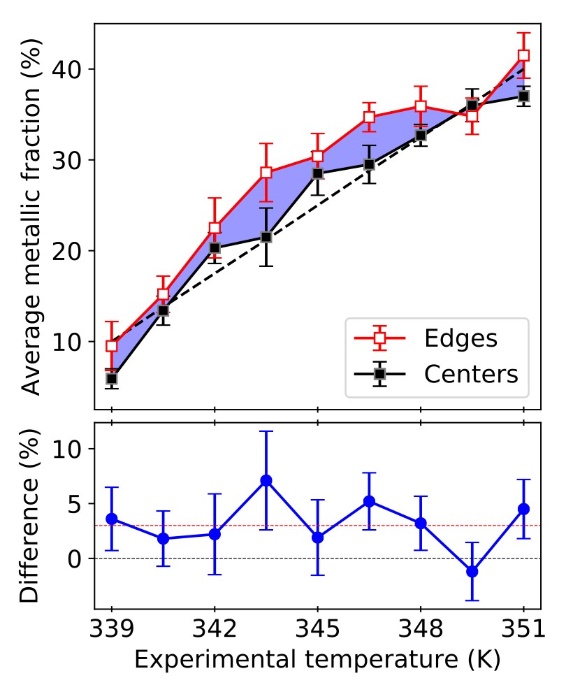 |
| The plot for specialists: During the transition from the non-conducting to the conducting state, the conducting fraction at the edges (top, red curve) is higher than in the centres of the samples (black curve), on average by three percent (bottom graph). (Image: DESY, Jan Schunck)
|
|
“In the future, such studies with improved spatial resolution in combination with the high brilliance of PETRA IV will be able to characterize size effects in microscopic functional materials and maybe even in small devices under in operando conditions. For example, we could observe a VO2-based transistor in action,” concludes Martin Beye.
|

