| Apr 12, 2023 |
Researchers find the key to overcome the limits in X-ray microscopy
(Nanowerk News) X-ray microscopes have the advantage of penetrating most substances, so internal organs and skeletons can be observed non-invasively through chest X-rays or CT scans. Recently, studies to increase the resolution of X-ray imaging technology are being actively conducted in order to precisely observe the internal structure of semiconductors and batteries at the nanoscale.
|
|
KAIST announced that a joint research team led by Professor YongKeun Park of the Department of Physics and Dr. Jun Lim of the Pohang Accelerator Laboratory has succeeded in developing a core technology that can overcome the resolution limitations of existing X-ray microscopes.
|
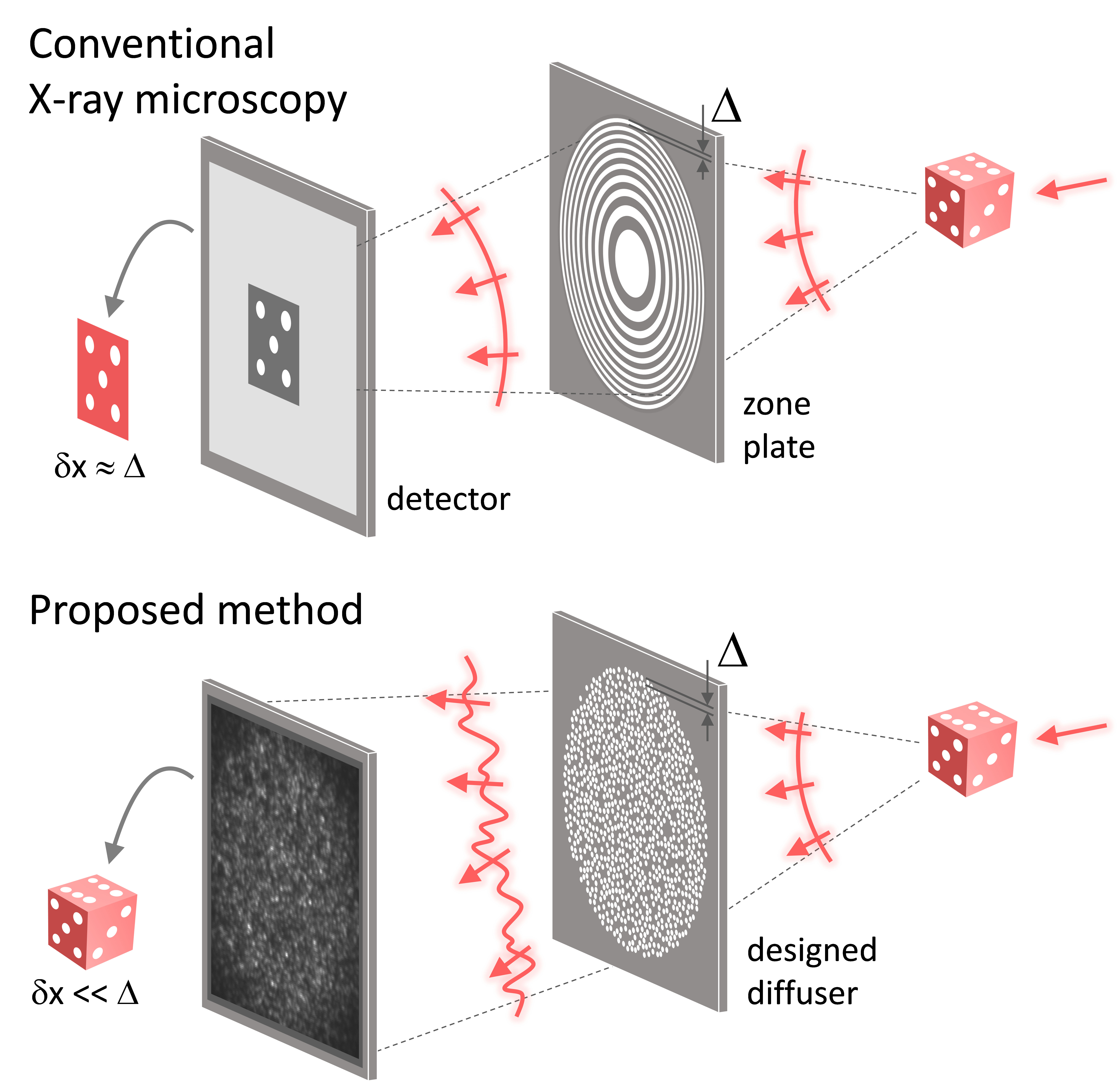 |
| Fig. 1. Designed diffuser as X-ray imaging lens. a, Schematic of full-field transmission X-ray microscopy. The attenuation (amplitude) map of a sample is measured. The image resolution (dx) is limited by the outermost zone width of the zone plate (D). b, Schematic of the proposed method. A designed diffuser is used instead of a zone plate. The image resolution is finer than the hole size of the diffuser (dx << D). (Image: KAIST)
|
|
This study, in which Dr. KyeoReh Lee participated as the first author, was published in Light: Science and Application ("Direct high-resolution X-ray imaging exploiting pseudorandomness").
|
|
X-ray nanomicroscopes do not have refractive lenses. In an X-ray microscope, a circular grating called a concentric zone plate is used instead of a lens. The resolution of an image obtained using the zone plate is determined by the quality of the nanostructure that comprises the plate. There are several difficulties in fabricating and maintaining these nanostructures, which set the limit to the level of resolution for X-ray microscopy.
|
|
The research team developed a new X-ray nanomicroscopy technology to overcome this problem. The X-ray lens proposed by the research team is in the form of numerous holes punched in a thin tungsten film, and generates random diffraction patterns by diffracting incident X-rays. The research team mathematically identified that, paradoxically, the high-resolution information of the sample was fully contained in these random diffraction patterns, and actually succeeded in extracting the information and imaging the internal states of the samples.
|
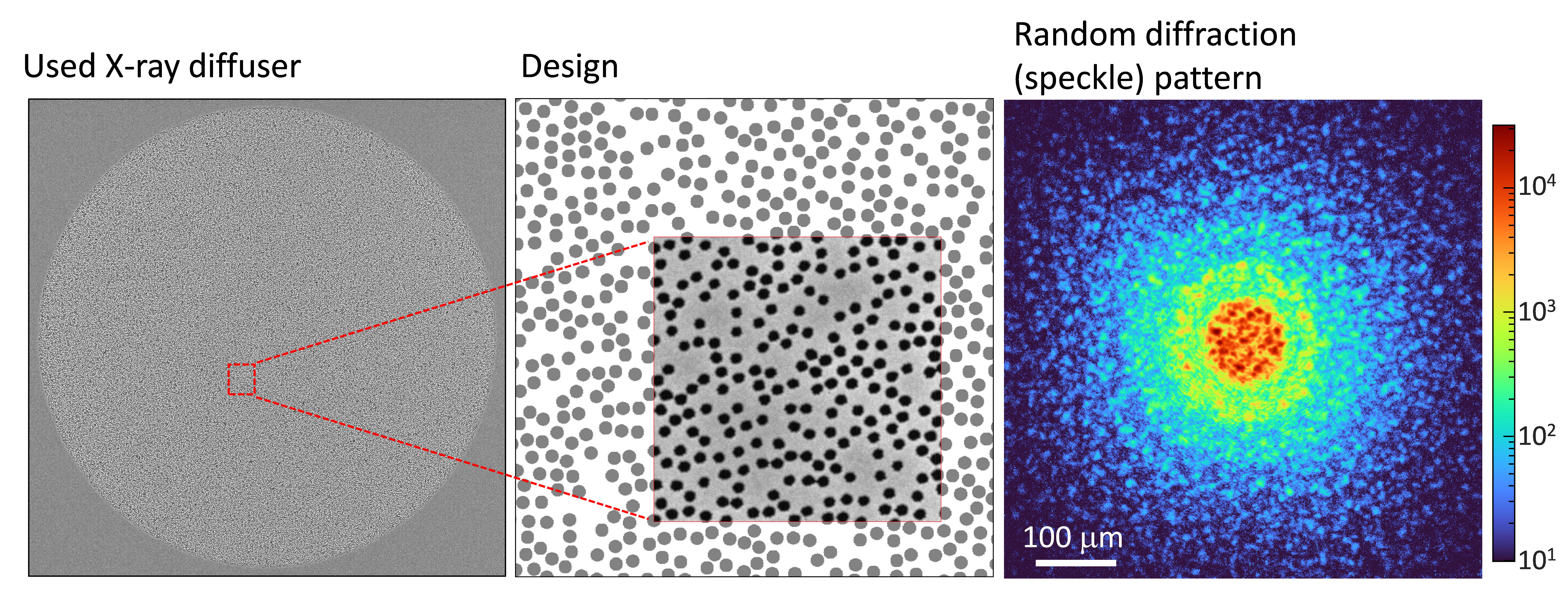 |
| Fig. 2. The left panel is a surface electron microscopy (SEM) image of the X-ray diffuser used in the experiment. The middle panel shows the design of the X-ray diffuser, and there is an inset in the middle of the panel that shows a corresponding part of the SEM image. The right panel shows an experimental random X-ray diffraction pattern, also known as a speckle pattern, obtained from the X-ray diffuser. (Image: KAIST)
|
|
The imaging method using the mathematical properties of random diffraction was proposed and implemented in the visible light band for the first time by Dr. KyeoReh Lee and Professor YongKeun Park in 2016 (Nature Communications, "Exploiting the speckle-correlation scattering matrix for a compact reference-free holographic image sensor"). This study uses the results of previous studies to solve the difficult, lingering problem in the field of the X-ray imaging.
|
|
The resolution of the image of the constructed sample has no direct correlation with the size of the pattern etched on the random lens used. Based on this idea, the research team succeeded in acquiring images with 14 nm resolution (approximately 1/7 the size of the coronavirus) by using random lenses made in a circular pattern with a diameter of 300 nm.
|
|
The imaging technology developed by this research team is a key fundamental technology that can enhance the resolution of X-ray nanomicroscopy, which has been blocked by limitations of the production of existing zone plates.
|
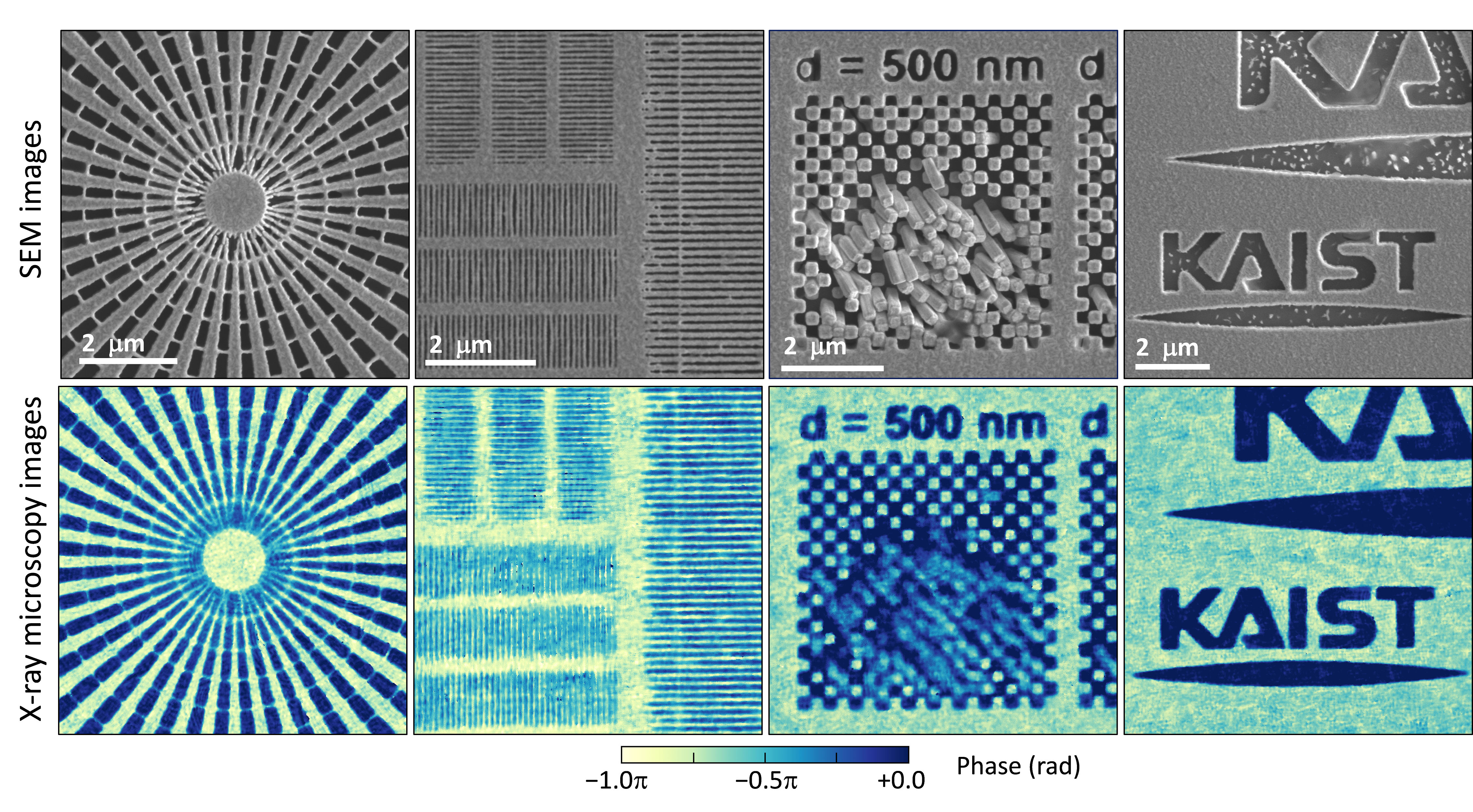 |
| Fig. 3. Images taken from the proposed randomness-based X-ray imaging (bottom) and the corresponding surface electron microscope (SEM) images (top). (Image: KAIST)
|
|
The first author and one of the co-corresponding author, Dr. KyeoReh Lee of KAIST Department of Physics, said, ???In this study, the resolution was limited to 14 nm, but if the next-generation X-ray light source and high-performance X-ray detector are used, the resolution would exceed that of the conventional X-ray nano-imaging and approach the resolution of an electron microscope.??? and added, ???Unlike an electron microscope, X-rays can observe the internal structure without damaging the sample, so it will be able to present a new standard for non-invasive nanostructure observation processes such as quality inspections for semiconductors.???.
|
|
The co-corresponding author, Dr. Jun Lim of the Pohang Accelerator Laboratory, said, ???In the same context, the developed image technology is expected to greatly increase the performance in the 4th generation multipurpose radiation accelerator which is set to be established in Ochang of the Northern Chungcheong Province.???
|

