| Oct 05, 2023 |
Successful morphing of inorganic perovskites without damaging their functional properties
(Nanowerk News) A research team co-led by scholars from City University of Hong Kong (CityU) has successfully morphed all-inorganic perovskites at room temperature without compromising their functional properties. Their findings demonstrate the potential of this class of semiconductors for manufacturing next-generation deformable electronics and energy systems in the future.
|
|
All-inorganic lead halide perovskites are becoming increasingly important semiconducting materials in energy conversion and optoelectronics because of their outstanding performance and enhanced environmental stability.
|
|
“However, unlike metal materials or polymers, inorganic semiconductors are often brittle and hard to process. This strongly restricts their applications as optoelectronic products that must withstand mechanical stress and strain without losing their functionality,” said Professor Chen Fu-Rong, Associate Vice-President (Mainland Collaboration) and Chair Professor of Materials Science at CityU, who co-led the study (Nature Materials, "Multislip-enabled morphing of all-inorganic perovskites").
|
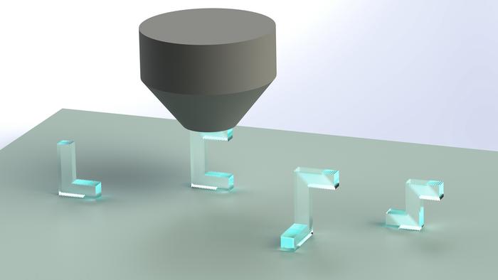 |
| Morphing of all-inorganic perovskite micropillars into distinct geometries through multislip. (Image: Dr Li Xiaocui / City University of Hong Kong)
|
|
To overcome this limitation, a research team led by Professor Chen, along with Professor Johnny Ho Chung-yin, Associate Head and Professor in the Department of Materials Science and Engineering (MSE), Professor Zhao Shijun, in the Department of Mechanical Engineering (MNE) at CityU, and Professor Lu Yang, former professor in MNE and currently working at The University of Hong Kong (HKU), explored the deformability of all-inorganic perovskites (CsPbX3, where X can be Cl, Br or I ions). They found perovskites can be substantially morphed into distinct geometries at room temperature while preserving their functional properties, an achievement unprecedented in conventional inorganic semiconductors.
|
|
In their experiments, the team first synthesized single-crystal micropillars of CsPbX3 with diameters and widths ranging from 0.4 to 2 µm and lengths of 3 to 10 µm, using the vapour-liquid-solid method. They then conducted in situ compression experiments with a scanning electron microscope.
|
|
They found that under compression, there were continuous slips of partial dislocations on multiple slip systems in the CsPbX3 crystal lattice. This ‘domino-like’ multi-slipping deformation mechanism enabled the micropillars to deform into various distinct shapes without fracturing, including upside-down L shape, Z shape, and wine-glass shape.
|
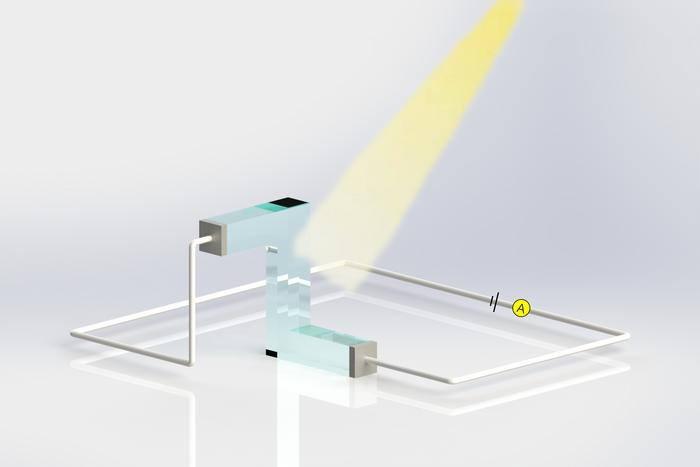 |
| Applying morphed perovskites to construct an innovative photodetector. (Image: Dr Li Xiaocui / City University of Hong Kong)
|
|
With the aid of an atomic-resolution transmission electron microscope (TEM), the team revealed that the atoms in the deformation zone were well connected, leading to undamaged functional properties. “We also observed that the optoelectronic performance of the micropillars remained unaffected by the deformation,” said Professor Ho. “This demonstrates the potential of these materials for use in deformable optoelectronics.”
|
|
The research team performed further electronic and structural analyses to uncover the physical origin of this unusual behaviour. “The secret of the morphing ability is the low-slip energy barrier, which ensures facile slips, and the strong Pb–X bonds, which maintain the crystal’s structural integrity and prevent cracking or cleaving,” said Professor Zhao Shijun, who specializes in the properties of computational materials. And the bandgap – an energy index influencing the total electrical properties of intrinsic semiconductors – of the CsPbX3 crystal lattice remained unchanged after deformation, indicating that the electronic structure of the material was unaffected, he added.
|
|
“Our results demonstrated that all-inorganic CsPbX3 single crystals can be substantially deformed and facilely morphed into various shapes through multi-slipping under ambient conditions, without changing their crystalline integrity, lattice structure or optoelectronic properties,” said Professor Chen.
|
|
“This achievement represents a significant step towards designing and manufacturing innovative energy devices and deformable electronics. The underlying mechanism, uncovered by a TEM at the atomic level provides important implications for seeking other intrinsic ductile semiconductors,” he added.
|

