| Oct 17, 2023 |
Scientists demonstrate ultrafast photoemission from carbon nanotube emitter
(Nanowerk News) A joint research team led by Prof. DAI Qing and Prof. LI Chi from the National Center for Nanoscience and Technology (NCNST) of the Chinese Academy of Sciences (CAS) has demonstrated the coherent ultrafast photoemission from a single quantized energy level of a carbon nanotube.
|
|
The study was published in Science Advances ("Coherent ultrafast photoemission from a single quantized state of a one-dimensional emitter").
|
Key Takeaways
|
|
Researchers have achieved ultrafast photoemission from a single energy level of a carbon nanotube.
Ultrafast electron pulses, with their high temporal and spatial resolution, are touted as the future of ultrafast characterization technology.
Traditional metal nanostructures suffer from significant energy dispersion; carbon nanotubes overcome this limitation.
By leveraging the atomic structure of carbon nanotubes, the team realized an electron source with lower energy spread and close to the time-energy uncertainty principle limit.
This breakthrough can lead to electron probes with unprecedented spatial and time resolution, enhancing applications like attosecond electron microscopy.
|
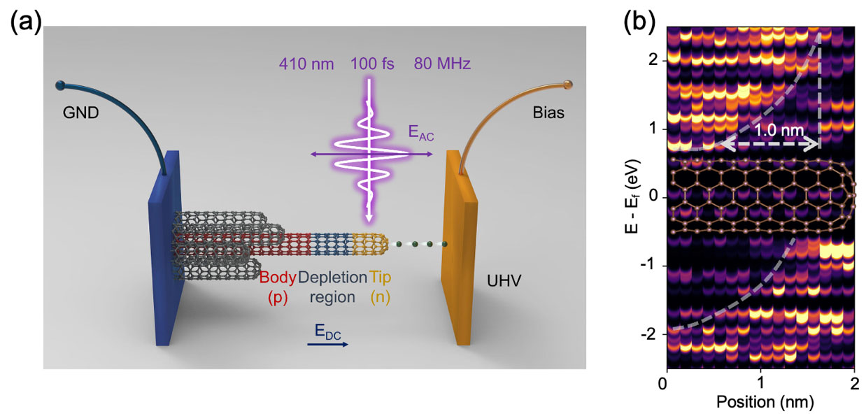 |
| Fig. 1 (a) Schematic diagram of ultrafast electron emission from carbon nanotubes. (b) TDDFT calculation results show that a depletion layer barrier can be formed at the tip of the carbon nanotube. (Image: NCNST)
|
The Research
|
|
Exploring dynamical processes at extreme spatiotemporal scales is pivotal for scientific and technological advancements. This is particularly true in the microscopic realm, where most movements are ultrafast, especially at the atomic spatial scale, since ultrafast processes can reach durations of a few femtoseconds or even attoseconds.
|
|
Compared with ultrafast light pulses, ultrafast electron pulses offer both high temporal and spatial resolution, making them a promising next-generation ultrafast characterization technology that could potentially exceed attosecond light pulses.
|
|
The monochromaticity of the electron source is vital for achieving high spatial resolution. However, the strong interaction between electrons and the optical field results in excited electrons occupying a wide range of energy levels. This leads to significant energy dispersion (>600meV) in ultrafast electron sources that rely on traditional metal nanostructures.
|
|
To address this issue, Prof. DAI's team proposed the use of carbon nanotubes as ultrafast electron source materials, replacing conventional metal nanostructures in their previous study.
|
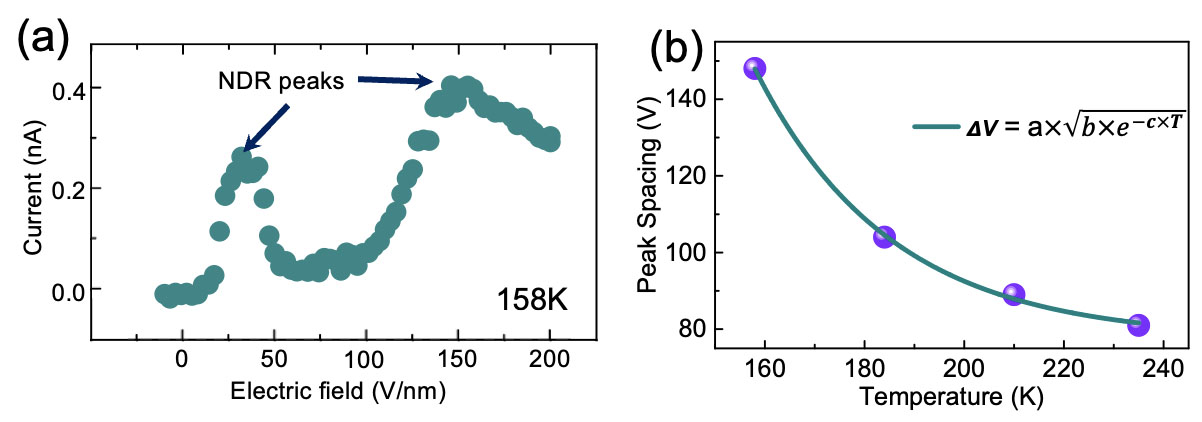 |
| Fig. 2 (a) Experimental observation of negative differential resistance in ultrafast electron emission. (b) The dependence of the peak-to-peak distance of the negative resistance peak on temperature. (Image: NCNST)
|
|
In the current study, the researchers used single-walled carbon nanotubes with a diameter of approximately 2nm as emitters, achieving ultrafast resonant tunneling single-electron emission.
|
|
They employed Time-Dependent Density Functional Theory (TDDFT) for simulation and discovered that a depletion layer barrier could form between the carbon nanotube's cap and its body. This, in conjunction with the vacuum barrier, forms a double barrier structure, enabling the zero-dimensional cap to serve as an electron resonant cavity, supporting both resonant tunneling and Coulomb blockade effects.
|
|
Subsequently, they finely tuned the double barrier structure at the tip by controlling the carrier concentration through operating the local temperature, and observed the phenomenon of laser-induced Negative Differential Resistance (NDR), proving the effect of resonant tunneling.
|
|
The adjustable peak distance of the negative resistance peak also suggested the presence of energy level renormalization in the cap, supporting the Coulomb blockade-controlled single-electron emission mechanism.
|
|
Furthermore, they observed the splitting phenomenon of the NDR peak. TDDFT simulations confirmed that this phenomenon is due to Stark splitting of two degenerate quantum states caused by the combined effect of the static field and laser field. This indicates that quantum energy levels can be further fine-tuned to achieve more controlled electron emission.
|
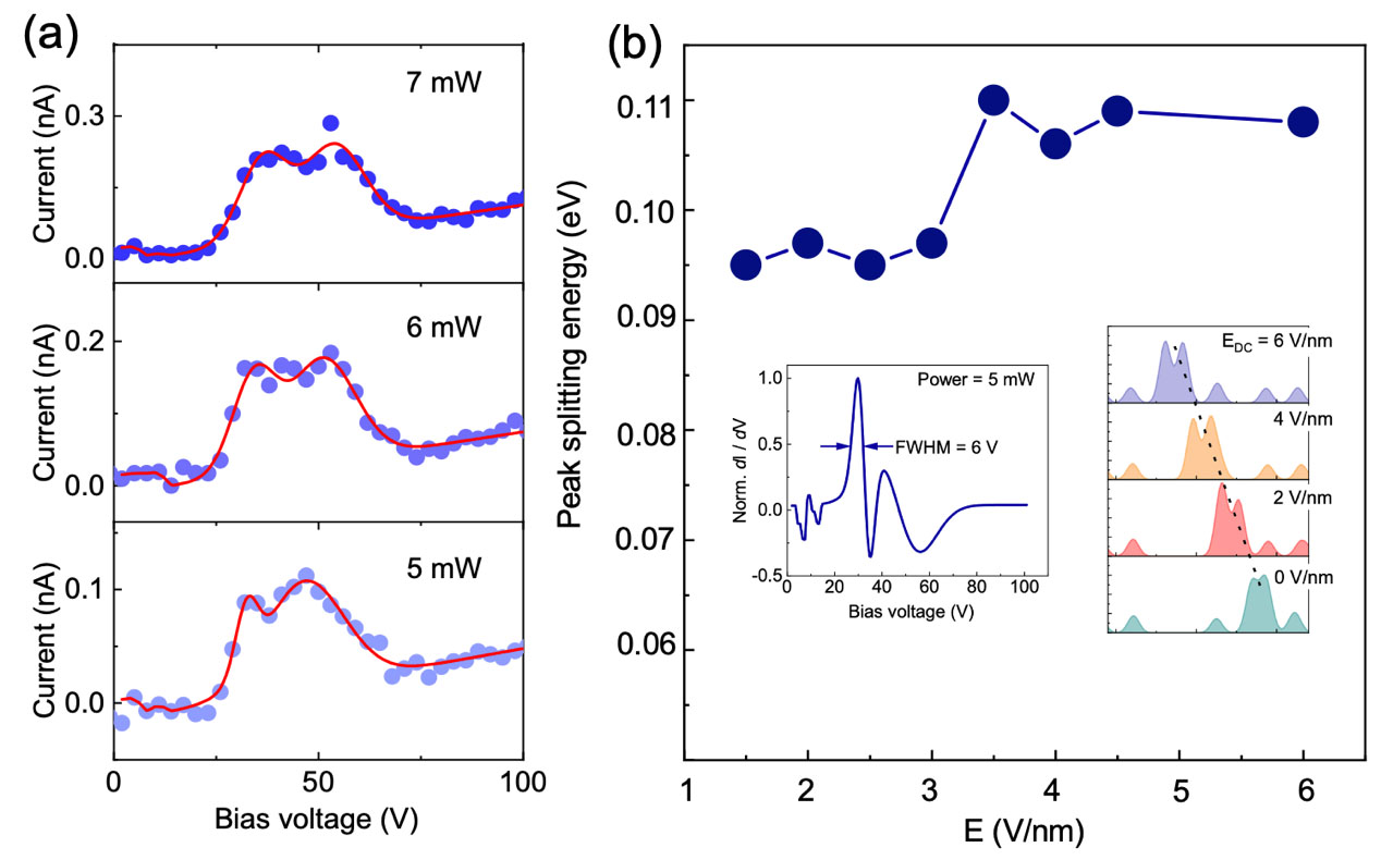 |
| Fig. 3 (a) Splitting phenomenon of the negative resistance peak. (b) Using TDDFT calculation, the energy value corresponding to the splitting is estimated to be about 110meV (corresponding to about 11.6V bias), and the electron emission energy spread is estimated to be about 57meV (corresponding to about 6V bias). (Image: NCNST)
|
|
By assessing the degree of energy level splitting and combining it with time-dependent first-principles calculations, it was estimated that the electron emission energy spread was approximately 57meV, which is an order of magnitude lower than that of metals.
|
|
"Utilizing the unique atomic structure of carbon nanotubes, it is possible to achieve an ultrafast coherent electron source close to the time-energy uncertainty principle limit," said Prof. DAI. "This could enable electron probes to have sub-angstrom spatial resolution and femtosecond time resolution, which is of great significance for many scientific and technological applications, including attosecond electron microscopy."
|

