| Dec 27, 2023 |
Researchers develop selective transfer printing technology for microLEDs(Nanowerk News) MicroLEDs are a light source for next-generation displays that utilize inorganic LED chips with a size of less than 100 µm. MicroLEDs have attracted a great deal of attention due to their superior electrical/optical properties, reliability, and stability compared to conventional displays such as LCD, OLED, and QD. |
| To commercialize microLEDs, transfer printing technology is essential for rearranging microLED dies from a growth substrate onto the final substrate with a desired layout and precise alignment. However, previous transfer methods still have many challenges such as the need for additional adhesives, misalignment, low transfer yield, and chip damage. |
| Professor Lee’s research team has developed a micro-vacuum assisted selective transfer printing (µVAST) technology to transfer a large number of microLED chips by adjusting the micro-vacuum suction force. |
| The research was published in Nature Communications ("Universal selective transfer printing via micro-vacuum force"). |
| The key technology relies on a laser-induced etching (LIE) method for forming 20 μm-sized micro-hole arrays with a high aspect ratio on glass substrates at fabrication speed of up to 7,000 holes per second. The LIE-drilled glass is connected to the vacuum channels, controlling the micro-vacuum force at desired hole arrays to selectively pick up and release the microLEDs. |
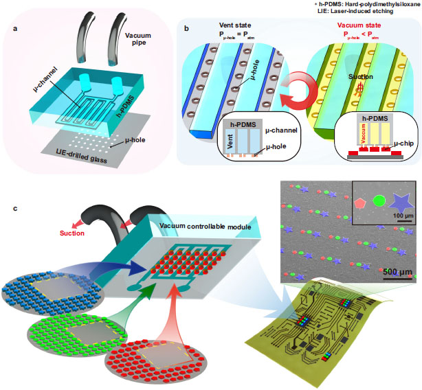 |
| Concept of micro-vacuum assisted selective transfer printing (μVAST). (Image: KAIST) |
| The micro-vacuum assisted transfer printing accomplishes a higher adhesion switchability compared to previous transfer methods, enabling the assembly of micro-sized semiconductors with various heterogeneous materials, sizes, shapes, and thicknesses onto arbitrary substrates with high transfer yields. |
| Professor Keon Jae Lee said, “The micro-vacuum assisted transfer provides an interesting tool for large-scale, selective integration of microscale high-performance inorganic semiconductors. Currently, we are investigating the transfer printing of commercial microLED chips with an ejector system for commercializing next-generation displays (Large screen TVs, flexible/stretchable devices) and wearable phototherapy patches.” |
| Source: KAIST (Note: Content may be edited for style and length) |

