| Jan 08, 2024 |
Substitutional doping of two-dimensional semiconductor for broadband photodetector(Nanowerk News) Substitutional doping from foreign elements stands out as a preferred method for precisely tailoring the electronic band structure, conduction type, and carrier concentration of pristine materials. In the realm of three-dimensional (3D) monocrystalline silicon, for instance, the introduction of boron (B) and nitrogen (N) atoms as acceptor and donor dopants, respectively, has proven highly effective in enhancing carrier mobility. This improvement positions silicon for advanced applications in integrated circuits. |
| Expanding into the realm of two-dimensional (2D) semiconductors, molybdenum disulfide (MoS2) holds immense potential for future optoelectronic devices. However, the controllable doping strategies for 2D materials and their prospective application directions necessitate further exploration. As a new frontier in materials science, the quest for optimal doping methodologies in 2D materials continues to unfold, paving the way for unprecedented advancements in the field of optoelectronics. |
| Researchers led by Anlian Pan, Dong Li and Shengman Li from Hunan University, China, are dedicated to pioneering the synthesis of large-area, high-quality, and low-defect-density two-dimensional semiconductors. Their research focuses on unraveling the photoelectric properties of these materials and exploring their potential in future device applications. |
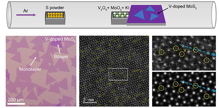 |
| V-doped MoS2 monolayer is achieved through chemical vapor deposition method. (©Frontiers of Optoelectronics) |
| Building on the foundation of preparing high-mobility pure MoS2, the researchers delved into the realm of foreign substitutional doping, introducing vanadium (V) atoms. Their approach aimed to fine-tune the transfer characteristics of MoS2 by varying the V doping concentration. Notably, their investigations revealed that V-doped MoS2 monolayers with low doping concentrations exhibited enhanced B-exciton emission, showcasing promise for applications in broadband photodetectors. |
| This work was published in Frontiers of Optoelectronics ("Vapor growth of V-doped MoS2 monolayers with enhanced B-exciton emission and broad spectral response"). This research contributes valuable insights to the evolving landscape of two-dimensional semiconductors and their potential impact on optoelectronic technologies. |
| Source: Frontiers Journal (Note: Content may be edited for style and length) |

