| May 07, 2024 |
Adjustment methods of Schottky barrier height in one- and two-dimensional semiconductor devices(Nanowerk News) In a paper published in Science Bulletin ("Adjustment methods of Schottky barrier height in one- and two-dimensional semiconductor devices"), an international team of scientists present a comprehensive overview of the static and dynamic adjustment methods of Schottky barrier height, with a particular focus on the recent advancements in nano-semiconductor devices. These methods encompass the work function of the metals, interface gap states, surface modification, image-lowering effect, external electric field, light illumination, and piezotronics effect. |
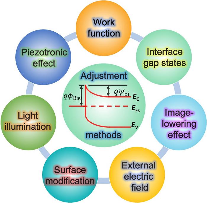 |
| In this picture, researchers summarize the commonly used methods for adjusting the Schottky barrier, including the work function of the metals, interface gap states, image lowering effect, external electric field, surface modification, light illumination, and piezotronic effect. (Image: Jianping Meng) |
| This review is organized by Prof. Jianping Meng and Zhou Li (Beijing Institute of Nanoenergy and Nanosystems, Chinese Academy of Sciences) and Prof. Chengguo Lee (Department of Electrical and Computer Engineering, National University of Singapore). The review provides an overview of static and dynamic approaches for adjusting Schottky barrier height (SBH). Static approaches include metal selection and interface engineering. Dynamic adjustment techniques for the SBH include surface modification, image-force lowering, external electric field application, light illumination, and the piezotronic effect. |
| The review also discusses strategies to overcome the Fermi level pinning effect induced by interface gap states. The inevitable Fermi level pinning caused by interface gap states makes it difficult to eliminate Schottky barriers. An effective method to eliminate Fermi level pinning is to form van der Waals contacts in 2D material-based devices. |
| However, the existence of a gap introduces a non-negligible tunnel barrier, leading to high contact resistance and low charge injection efficiency. To overcome the tunnel barrier, methods such as edge contacts, semi-metal contacts, ultrahigh vacuum evaporation, low-energy metal integration, and hybridization of metal-semiconductor (M-S) energy bands at the Fermi energy have been developed. |
| Although these methods can reduce or eliminate the tunnel barrier, their limited industrial compatibility restricts their widespread application. Therefore, further efforts are needed to develop industry-compatible technologies that meet the evolving needs of the semiconductor industry. |
| Source: Science China Press (Note: Content may be edited for style and length) |

