| Posted: July 14, 2009 |
Promising results in the race to scale CMOS to 22nm and below |
|
(Nanowerk News) IMEC has achieved promising results in the race to scale CMOS to 22nm and below. The breakthroughs from its transistor scaling programs include a successful integration of the laser-anneal technique in a high-K/metal-gate first process and a step forward towards fabricating aggressively scaled germanium-pFET transistors.
|
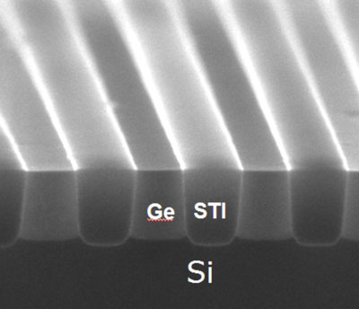 |
| X-SEM picture of the Ge-in-STI structure.
|
|
To scale CMOS technology to 22nm and below, high permittivity dielectrics and metal gates (Hk/MG) are considered as one of the best options. One Hk/MG integration scheme is metal inserted poly-silicon (MIPS). With a MIPS
|
|
CMOS process flow, IMEC has compared spike anneal and laser anneal. For the first time, IMEC has shown functional ring oscillators with millisecond anneal-only that show a similar performance as oscillators made using spike anneal.
|
|
The major advantage of using laser anneal over spike anneal is the reduced thermal budget. This limits the diffusion of dopants in the Si during their activation. Such a limited diffusion helps to keep short channel effects under control as the physical dimensions of the transistors shrink. But laser anneal is also challenging. IMEC’s results point to optimizations of the process that limit the defects, maintain a low gate resistance, and show an excellent effective work-function control using high-K capping layers. Capping layers are dielectric layers that are deposited between the bulk dielectric and the metal gate to tune the effective work function of the electrode to the desired type (n- or p-).
|
|
Another scaling option that has attracted a lot of attention is using high-mobility materials to boost the carrier mobility of the MOS transistors, as this can lead to higher drive currents. This search has led to an interest in Germanium MOSFETs: it has proved possible to make Ge pFET devices with a hole mobility that is substantially above the hole mobility curve of silicon, and with conventional processes. IMEC’s research now shows, for the first time, an STI module (Shallow Trench Isolation) integrated in an advanced 70nm Ge-pFET technology allowing EOT in inversion scaling down to 0.85nm. IMEC has also made an in-depth analysis of the mechanisms that limit the hole mobility for sub-nm EOT Ge pFETs. These results pave the way for further optimizations of Ge pFET devices, and for their introduction in high-end high-performance ICs.
|
|
These results were obtained in cooperation with IMEC’s key parners in its core programs: Intel, Micron, Panasonic, Samsung, TSMC, Elpida, Hynix, Powerchip, Infineon, NXP, Qualcomm, Sony, ST Microelectronics. This work is further supported by the European collaborative projects, especially DUALLOGIC.
|
|
|
|
About IMEC
|
|
IMEC is a world-leading independent research center in nanoelectronics and nanotechnology. IMEC vzw is headquartered in Leuven, Belgium, has a sister company in the Netherlands, IMEC-NL, offices in the US, China and Taiwan, and representatives in Japan. Its staff of more than 1650 people includes about 550 industrial residents and guest researchers. In 2008, its revenue (P&L) was EUR 270 million.
|
|
IMEC’s More Moore research aims at semiconductor scaling towards sub-32nm nodes. With its More than Moore research, IMEC looks into technologies for nomadic embedded systems, wireless autonomous transducer solutions, biomedical electronics, photovoltaics, organic electronics and GaN power electronics.
|
|
IMEC’s research bridges the gap between fundamental research at universities and technology development in industry. Its unique balance of processing and system know-how, intellectual property portfolio, state-of-the-art infrastructure and its strong network worldwide position IMEC as a key partner for shaping technologies for future systems.
|

