| Posted: November 4, 2009 |
Silicon nanowires shorter than 3 nm could lose their intrinsic electronic characteristics |
| (Nanowerk News) The electronic properties of silicon nanowires (SiNW) have led to their application in a variety of devices, such as chemical and biological sensors, field-effect transistors, lithium batteries and photovoltaic cells. Of late, recent work has been focused on scaling down the size of these devices, resulting in research on even smaller nanowires. SiNWs as thin as 1 nm diameter with <112> growth orientation have been synthesized, or in the case of <110> growth orientation, theoretically predicted. It is therefore crucial to understand the electron transport properties of such ultra-thin nanowires before they can be adopted into applications. |
| Now, researchers from Singapore and China, led by Man-Fai Ng and Shuo-Wang Yang of A*STAR’s Institute of High Performance Computing, have used a combined theoretical approach of density functional theory (DFT) and non-equilibrium Green’s function (NEGF) to study the effects of length, growth orientation and surface reconstruction on the conducting characteristics of ultrathin SiNWs ("Geometry Dependent I-V Characteristics of Silicon Nanowires"). |
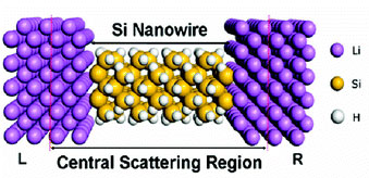 |
| Fig. 1: The two-probe model that is used to simulate the I–V curves of the SiNWs. |
| The current–voltage (I–V) characteristics of such nanowires can be investigated by calculating their conductance and I–V curves. Factors such as surface defects, disorder or doping have been considered, but such studies have mostly used the tight-binding or empirical methods. Although thinner SiNWs have also been investigated through ab initio studies, most of them do not include metal electrodes explicitly in their calculations, nor take into account the fact that in such devices, the wires are attached to two electrodes. |
| The researchers studied the I–V characteristics of hydrogenated SiNWs with four different growth orientations as well as samples with modified surfaces (Fig. 1). All the nanowires studied have diameters of approximately 1 nm and lengths of between 0.6 and 3.3 nm, and are attached at each end to a metal electrode. The effect of the metal/semiconductor surface mismatch was also investigated by testing electrodes with either (110) or (100) surfaces. |
| With such short nanowires, the researchers observed a strong tunneling effect caused by the very close proximity of the electrodes and by the mismatch at the surface contacts. However, for SiNWs that are longer than 3 nm in length, the tunneling effect was significantly reduced and the nanowires resume their intrinsic I–V curves. For the surface modified nanowires, the conductance was enhanced, suggesting the presence of conducting channels on the surface. |
| These results are in good agreement with the unexpectedly high conductance recently observed experimentally for large undoped SiNWs with a diameter of ca. 70 nm, which was also explained as due to surface effects. |
| Source: A*STAR |

