| Posted: November 12, 2009 |
Bowtie-shaped antennae function as the first tunable nano colorsorters |
|
(Nanowerk News) Looking sharp and looking for light - Berkeley Lab researchers have engineered a new class of bowtie-shaped devices that capture, filter and steer light at the nanoscale. These “nano-colorsorter” devices act as antennae to focus and sort light in tiny spaces, a useful technique for harvesting broadband light for color-sensitive filters and detectors.
|
|
Currently, optical fibers employ light to transport data with very high bandwidth, but the technique hits a roadblock as light is squeezed into smaller and smaller photonic circuits. This roadblock is the diffraction limit - a fundamental restriction in concentrating photons into regions smaller than half their wavelength. In contrast, electronic devices are readily fashioned at nanometer scales; however, electronic data transfer operates at frequencies far below those for fiber optics, with much lower bandwidth, reducing the amount of data carried.
|
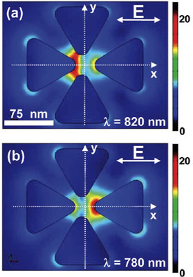 |
| This scanning electron image of a nano colorsorter with the vertical bowtie antenna shifted 5 nanometers (nm) to the left of center. In (a) the bowtie has been exited at 820 nm and in (b) at 780 nm. The two modes are spectrally and spatially distinct while maintaining nanoscale mode volumes.
|
|
This scanning electron image of a nano colorsorter with the vertical bowtie antenna shifted 5 nanometers (nm) to the left of center. In (a) the bowtie has been excited at 820 nm and in (b) at 780 nm. The two modes are spectrally and spatially distinct while maintaining nanoscale mode volumes.
|
|
A recent technology, coined “plasmonics, ” crowds electromagnetic waves into metal structures with dimensions much smaller than the wavelength of light for transmitting data at optical frequencies, marrying the best aspects of optical and electronic communications. A particularly promising class of structures for enhancing this crowding effect is nanoscale optical antennae made of gold, which leverage plasmonic behavior to efficiently capture and confine light in miniscule dimensions.
|
|
“Like the antenna on your TV or radio, optical nanoantennas efficiently catch and concentrate energy, but the wavelengths are much smaller,” says Jim Schuck, a staff scientist withn the Molecular Foundry, a U.S. Department of Energy (DOE) national user facility at Berkeley Lab that provides support to nanoscience researchers around the world.
|
|
“We’ve made the first engineered and nanofabricated stucture for nanoscale light distribution that can ship and manipulate ultra-confined optical information with a knob you can easily tune-the energy or color of light,” says Schuck, who works in the Foundry’s Imaging and Manipulation of Nanostructures Facility.
|
|
Molecular Foundry post-doctoral researcher Zhaoyu Zhang, working with Schuck and Nanofabrication Facility Director Stefano Cabrini, fabricated nanoantennas from four equilateral triangles of gold lithographically patterned to create a ‘cross’ geometry.
|
|
Breaking the symmetry of this cross-shaped device affects its primary resonance mode - a property best illustrated by the shattering of a champagne flute when it encounters a musical tone of the right pitch. In these cross nanoantennas, the resonant modes correspond to different frequencies, or colors, of light.
|
|
“We can now control the plasmonic properties of these devices by introducing asymmetry, and we find red and blue light is literally sent left and right,” says Zhang. “By pushing the limits of manipulating light in a smaller volume, we can move information to one place or another quickly and efficiently, which is important for fast, color-sensitive photodetection. ”
James Schuck and Zhaoyu Zhang at the Molecular Foundary fabricated nano-sized antennae from four equilateral triangles of gold that were lithographically patterned to create a “cross” geometry. These bowtie-shaped antennae function as nano colorsorters, able to capture, filter and steer light at the nanoscale.
|
|
Indeed, shifting the vertically aligned bowtie in the cross nanoantenna just five nanometers left of center generates two resonance modes, producing a two-color filter. The team further demonstrated this effect by breaking other symmetries of the bowties, leading to a three-color filter. This symmetry breaking gives scientists the ability to “auto-tune” a device to a desired set of colors or energies, crucial for filters and other detectors. Using the nanofabrication capabilities available at the Foundry, the scientists plan to explore adjusting the size, shape, and position of the bowties to optimize device properties. For example, thousands of bowties could be packed in an area less than one millimeter across, enabling large, but ultrafast, detector arrays.
|
|
“Our findings lend insight into the link between simple symmetry breaking and the coherent coupling properties of localized plasmons, providing a pathway for engineering intricate devices that can control light in extremely confined spaces,” Schuck adds.
|
|
A scientific paper reporting this research entitled “Manipulating nanoscale light fields with the asymmetric bowtie nano-colorsorter,” by Zhaoyu Zhang, Alexander Weber-Bargioni, Shiwei Wu, Scott Dhuey, Stefano Cabrini and James Schuck, appears in Nano Letters and is available in Nano Letters online.
|
|
Work at the Molecular Foundry was supported by the Director, Office of Science, Office of Basic Energy Sciences, Division of Materials Science and Engineering, of the DOE under Contract No. DE-AC02-05CH11231.
|
|
The Molecular Foundry is one of the five DOE Nanoscale Science Research Centers (NSRCs), premier national user facilities for interdisciplinary research at the nanoscale. Together the NSRCs comprise a suite of complementary facilities that provide researchers with state-of-the-art capabilities to fabricate, process, characterize and model nanoscale materials, and constitute the largest infrastructure investment of the National Nanotechnology Initiative. The NSRCs are located at DOE’s Argonne, Brookhaven, Lawrence Berkeley, Oak Ridge and Sandia and Los Alamos National Laboratories.
|
|
Berkeley Lab is a U.S. Department of Energy national laboratory located in Berkeley, California. It conducts unclassified scientific research for DOE’s Office of Science and is managed by the University of California.
|

