| Posted: November 19, 2009 |
Nanoelectronics researchers demonstrate repulsive and attractive nanophotonic forces |
|
(Nanowerk News) The University of Ghent and the nanoelectronics research center IMEC demonstrated repulsive and attractive nanophotonic forces, depending on the spatial distribution of the light used ("Tunable optical forces between nanophotonic waveguides"). These fundamental research results might have major consequences for telecommunication and optical signal processing.
|
|
Photon impulse is usually considered to be relatively weak. In our macroscopic world, photons bumping into an object exert an almost negligible force on this object. Nevertheless, this picture changes dramatically when the object size is shrunk to nanoscale dimensions. When light is confined to very small cross-sections and large gradients exist in the spatial field distribution of the light, the optical gradient force induced per photon increases dramatically.
|
 |
|
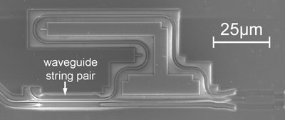
Using advanced fabrication technologies, including DUV (Deep Ultraviolet) lithography and critical-point-drying, the researchers created two parallel waveguides on a silicon-on-insulator chip. The waveguides are freestanding, acting as movable strings. They have a width of 445nm, a height of 220nm, a length of approximately 25µm and they are separated by a 220nm gap.
|
|
By sending laser light through the waveguides the researchers generated optical forces between them. Depending on the spatial distribution of the light (both in amplitude and phase) the strings were attracting or repulsing each other. The repulsive force that had never been demonstrated before makes this experiment of fundamental scientific importance.
|
|
The experiment might eventually have a major impact to achieve very high speed telecommunication for optical forces provide an interesting option for implementing all-optical signal processing functions on a chip. All-optical routing is one of the key challenges in developing faster communication networks (such as the internet) and the new technique opens up new routes towards solutions for this bottleneck.
|
|
About IMEC
|
|
IMEC is a world-leading independent research center in nanoelectronics and nanotechnology. IMEC vzw is headquartered in Leuven, Belgium, has a sister company in the Netherlands, IMEC-NL, offices in the US, China and Taiwan, and representatives in Japan. Its staff of more than 1650 people includes about 550 industrial residents and guest researchers. In 2008, its revenue (P&L) was EUR 270 million.
|
|
IMEC’s More Moore research aims at semiconductor scaling towards sub-32nm nodes. With its More than Moore research, IMEC looks into technologies for nomadic embedded systems, wireless autonomous transducer solutions, biomedical electronics, photovoltaics, organic electronics and GaN power electronics.
|
|
IMEC’s research bridges the gap between fundamental research at universities and technology development in industry. Its unique balance of processing and system know-how, intellectual property portfolio, state-of-the-art infrastructure and its strong network worldwide position IMEC as a key partner for shaping technologies for future systems.
|

