| Posted: December 7, 2009 |
Microscopic gyroscopes, the key for motion sensing |
|
(Nanowerk News) Most people know what a gyroscope is and probably played with one as a child. Get the centre ring revolving at high speed using a length of string or piece of plastic, put the frame on a stand and watch it apparently defy gravity.
|
|
But as well as being one of the most enduring toys of the past century, the gyroscope has many practical applications. The first was as a gyrocompass for shipping, replacing traditional, less reliable, magnetic compasses, and then as a stabiliser in ships and aircraft and more recently spacecraft.
|
|
In recent times, the focus has switched to attempts to miniaturise gyroscopes, or to reproduce the gyroscopic effect in very small structures, so as to provide mass-market applications to consumers.
|
|
The aim was partially achieved with the development of tiny MEMS (micro-electro-mechanical system) gyroscopes. However, in order for them to have mass commercial potential, it was necessary to come up with a way of securely and cost-effectively packaging them to insulate and protect them from the external environment.
|
|
The EU-funded DAVID project was set up to do just this, with six partners from five countries looking at ways to reduce assembly and packaging costs for mass-produced hybrid integrated devices comprising both mechanical and electronic components.
|
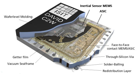 |
| The Chip-to-Wafer concept unites micromachined silicon sensors (top chip, shown as a transparent block) with a microelectronic chip (bottom). Within the ultra-small hermetic cavity between the chips, a getter film (black layer) covers the ASIC surface and provides a lifetime vacuum inside the package. This allows the sensor's proof mass to operate in a resonant mode with controlled damping. The chip stack is protected against fracturing by a wafer molding process. Through-silicon vias redistribute all contacts to solder balls on the backside, thus forming a chip-scale system in a package.
|
|
Bonding mechanical to electronics
|
|
The MEMS are bonded to electronic systems-on-chips or ASICs (application-specific integrated circuits), powerful micro-components which run devices such as mobile phones and gaming consoles. Large numbers of ASICs are mass produced by being “etched” onto silicon wafers in sophisticated, ultra-clean wafer fabrication plants.
|
|
Project coordinator Norman Marenco explains the challenge: “To create a gyroscope effect for measuring motion in a vehicle or even a pedestrian, you have to provide a moving structure inside a very, very small device and this means combining the mechanical movement with some very sophisticated electronics.
|
|
“As the device will be embedded in a vehicle electronics system, or even eventually a mobile phone, it needs to be self-contained and continue operating for many years.”
|
|
What this means is the moving parts will be oscillating continuously. In theory, they would ideally be in a vacuum so there is no resistance to the movement, but in practice a small amount of air pressure is needed to avoid disturbance so the conditions are near vacuum. To maintain this state indefinitely, strong and durable packaging which individually seals off each device is a must.
|
|
Wafer-level packaging approach
|
|
To create the devices, the MEMS are bonded directly onto ASICs resulting in very short interconnections between the mechanical and electronics structures to produce the best possible signal quality. The bonding can be done using either a chip-to-wafer (C2W) or wafer-to-wafer (W2W) approach, but due to the large number of chips per wafer the only cost-effective way to go into mass production is the latter and so this is what the researchers and industrial partners worked towards.
|
|
So complex was the procedure, but so promising the initial results, the project was given a six-month extension until mid-2009 with a final report being published in September, by which time full wafer samples had been produced. A mould tool for 6-inch wafers was developed and various mould compounds tried out to find the ideal encapsulation for the chips on the wafers.
|
|
Now the project has managed to prove it is possible to mass-produce the MEMS/ASIC devices and hermetically seal them, industrial partner STMicroelectronics, a major chip manufacturer, has started work on a high-volume manufacturing approach using W2W integration.
|
|
Mass-market applications
|
|
Marenco predicts that, by 2012, the MEMS gyroscopic devices could be in mass production, initially for mobile phone applications. “You could have tiny devices embedded in mobile handsets that respond to movements made by the users so it is possible to keep exact track of the movements of somebody walking around. For human-machine interfaces and personal navigation systems you need to be able to track motions in three dimensions very precisely, which is what these devices can do,” he says.
|
|
Another potential mass-market application is stabilisation systems for motor vehicles, although this is not something the project studied in any depth.
|
|
Funding has now been sought for a follow-up project to try and develop a broader base of sensors for a wider range of applications, such as automotive ones. “Most of the partners from DAVID want to continue down this path and concentrate more on applications now the initial proof-of-concept work has been done. We also want to get more equipment suppliers involved, companies making devices like endoscopes and night vision products,” he says.
|

