| Posted: February 3, 2010 |
Nanoparticle assembly: Bridging spheres |
| (Nanowerk News) A process to rival traditional lithography approaches, and which can be used to create microwire networks, is now a step closer to real applicability in future electronics. By optimizing the processing conditions for ‘evaporative lithography’, a research team from Singapore and Australia has maximized the connectivity and conductivity of the microwire networks that conduct electricity ("Particulate Templates and Ordered Liquid Bridge Networks in Evaporative Lithography"). |
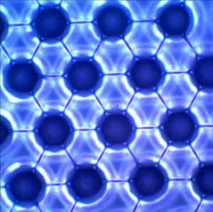 |
| Fig. 1: Micrograph view through the glass substrate showing the formation of a liquid bridge network during the evaporation of solvent. (Reproduced from Ref. 1 © 2009 The American Chemical Society) |
| “Evaporative lithography could offer a cost-effective and environmentally friendly bench-top alternative to existing lithographic techniques such as photolithography, soft lithography and nanoimprinting,” says team member Ivan Vakarelski from the A*STAR Institute of Chemical and Engineering Sciences, Singapore. He explains that the team is aiming primarily at creating large conducting microwire networks that, when deposited onto a glass substrate, could be used as transparent electrodes. These could be an alternative to the industry standard of indium tin oxide coatings, which would help circumvent the high cost and limited supply of indium. |
| Vakarelski and his co-workers created the microwire networks from solutions of gold nanoparticles of 20 nanometers diameter. As in their earlier work ("Assembly of Gold Nanoparticles into Microwire Networks Induced by Drying Liquid Bridges"), they first established a template of much larger latex microparticles on a substrate, then deposited solutions of the nanoparticles on top and allowed them to dry gradually. Surface tension then drove the solution into lines that formed ‘bridges’ between neighboring latex particles (Fig. 1). Once the pattern was completely dry and the researchers removed the latex particles, the gold nanoparticles from the solution remained in a network of microwires. |
| The network pattern depends on the original positioning of the latex particles in the template, allowing different microwire designs to be easily realized. Vakarelski and his co-workers found that the networks can be improved for maximum conductivity and connectivity by adding a surfactant and treating the latex spheres with heat and oxygen plasma. They believe that these factors act to stabilize the latex spheres and the liquid bridges during drying to encourage full microwire networks to form. |
| Vakarelski is optimistic that the technique will progress to a level such that it will be used in manufacturing processes. He explains that this can be achieved by adapting the template production and expanding the size capacity to the scale of silicon wafers used in electronics. |
| The team’s approach potentially has broader applications beyond electronics. “We can create special functional networks using semiconducting particles,” Vakarelski says. Other examples include magnetic particles, carbon nanotubes, DNA, proteins and other macromolecules and even mixtures of these to create networks and nodes with desired properties. |
| Source: Reprinted with permission from A*STAR |

