| Posted: February 17, 2010 |
Quantum effects must be taken into account in design of nanowires |
| (Nanowerk News) Silicon nanowires are a leading candidate for use in next-generation transistors because they allow for high densities and speeds, as well as low operating power. Numerical modeling is a key part of nanowire transistor design. However, the modeling of capacitance, an important transistor characteristic, has so far been based on semi-classical physics, rather than quantum physics. Now, Sai Kong Chin of the A*STAR Institute of High Performance Computing and co-workers at A*STAR and the National University of Singapore have developed a rigorous two-dimensional quantum model of the ‘gate-all-around’ nanowire configuration, leading to a better match with experimental data and highlighting the importance of quantum effects ("Self-Consistent SchrÖdinger–Poisson Simulations on Capacitance–Voltage Characteristics of Silicon Nanowire Gate-All-Around MOS Devices With Experimental Comparisons"). |
| In nanowire transistors, the nanowire forms a channel through which current flow is controlled by a gate electrode (Fig. 1). The best control has been demonstrated for the gate-all-around configuration, in which the gate wraps around the nanowire. The degree of gate control is critical to transistor function, and is determined in part by the nanowire capacitance. |
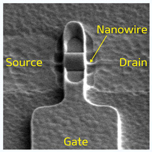 |
| Fig. 1: A single nanowire connecting source and drain contacts is wrapped by a cylindrical gate, which controls its current. (Reproduced from Ref. 1 © 2009 IEEE) |
| Accurate modeling of capacitance requires consideration of the quantum behavior of the wave-like electrons inside the nanowire, which Chin and co-workers accomplished by applying the Schrödinger–Poisson equation to the problem. They calculated the capacitance of the nanowire as a function of the gate electrode voltage, and compared the result to experimental measurements for nanowires of 9–10 nanometers in radius. |
| The capacitances calculated using semi-classical models were 10–20% higher than the experimental observations. The results of the quantum model, however, matched the experiments with good accuracy, demonstrating that quantum effects cannot be ignored at this size scale, serving to reduce the capacitance below what would be expected from purely geometric considerations. Furthermore, the quantum model properly reproduced variations in the capacitance that can be used to determine the energetic spectrum of states inside the nanowire, whereas semi-classical models could not. |
| The reduction of capacitance due to quantum effects complicates the design of future nanoscale devices. However, these effects give rise to a rich spectrum of states that may lead to new kinds of devices. In either case, modeling of this kind will prove useful. It may also be used in fields such as quantum liquids and strongly correlated systems, which are increasingly being studied as applications of nanowires. “Just as the ability to control and characterize two-dimensional electron gases in semiconductor heterostructures spurred advancement in mesoscopic physics in the past, I like to think that our effort in nanowires is part of a broader ‘sharpening of tools’ that may enable future breakthroughs,” says Chin. |
| Source: Reprinted with permission from A*STAR |

