| Posted: March 1, 2010 |
A simpler way to make micromachines |
|
(Nanowerk News) Microelectromechanical devices gave us the Wii and the digital projector. MIT researchers have found a way to manufacture them by stamping them on plastic, opening up the possibility of coating large areas with tiny sensors.
|
|
Microelectromechanical devices — tiny machines with moving parts — are everywhere these days: they monitor air pressure in car tires, register the gestures of video game players, and reflect light onto screens in movie theaters. Now, MIT researchers have discovered a way to manufacture them by stamping them onto a plastic film ("Contact-Printed Microelectromechanical Systems"). That should significantly reduce their cost, but it also opens up the possibility of large sheets of sensors that could, say, cover the wings of an airplane to gauge their structural integrity. The printed devices are also flexible, so they could be used to make sensors with irregular shapes. And since the stamping process dispenses with the harsh chemicals and high temperatures ordinarily required for the fabrication of microelectromechanical systems (MEMS), it could allow them to incorporate a wider range of materials.
|
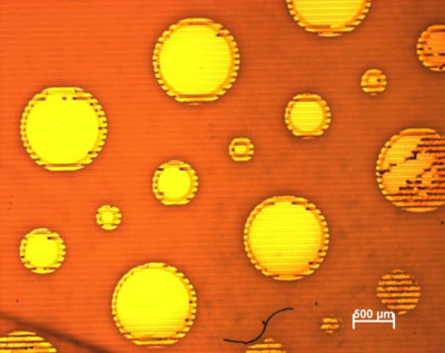 |
| To test a new technique for creating micromachines, MIT researchers deposited films of gold on a sheet of plastic; grooves in the plastic are visible as a series of horizontal lines. (Image: Corinne Packard and Apoorva Murarka)
|
|
Conventional MEMS are built through the same process used to manufacture computer chips, which is called photolithography: different layers of material are chemically deposited on a substrate — usually a wafer of some semiconducting material — and etched away to form functional patterns. Photolithography requires sophisticated facilities that can cost billions of dollars, so MEMS manufacture has high initial capital costs. And since a semiconductor wafer is at most 12 inches across, arranging today’s MEMS into large arrays requires cutting them out and bonding them to some other surface.
|
|
Besides serving as sensors to gauge the structural integrity of aircraft and bridges, sheets of cheap MEMS could also change the physical texture of the surfaces they’re applied to, altering the airflow over a plane’s wing, or modifying the reflective properties of a building’s walls or windows. A sheet of thousands of tiny microphones could determine, from the difference in the time at which sound waves arrive at different points, where a particular sound originated. Such a system could filter out extraneous sounds in a noisy room, or even perform echolocation, the way bats do. The same type of sheet could constitute a paper-thin loudspeaker; the vibrations of different MEMS might even be designed to interfere with each other, so that transmitted sounds would be perfectly audible at some location but inaudible a few feet away. The technology could also lead to large digital displays that could be rolled up when not in use.
|
|
How they did it
|
|
The MIT process begins with a grooved sheet of a rubbery plastic, which is coated with the electrically conductive material indium tin oxide. The researchers use what they call a “transfer pad” to press a thin film of metal against the grooved plastic. Between the metal film and the pad is a layer of organic molecules that weaken the metal’s adhesion to the pad. If the researchers pull the pad away fast enough, the metal remains stuck to the plastic.
|
|
“It’s kind of similar to if you have Scotch tape on a piece of paper,” says Corinne Packard, a postdoc in the Research Lab of Electronics at MIT who led the work, along with professors of electrical engineering Vladimir Bulovic and Martin Schmidt. “If you peel it off slowly, you can delaminate the tape very easily. But if you peel fast, you’ll rip the paper.”
|
|
Once the transfer pad has been ripped away, the metal film is left spanning the grooves in the plastic like a bridge across a series of ravines. Applying a voltage between the indium-tin-oxide coating and the film can cause it to bend downward, into the groove in the plastic: the film becomes an “actuator” — the moving part in a MEMS. Varying the voltage would cause the film to vibrate, like the diaphragm of a loudspeaker; selectively bending different parts of the film would cause them to reflect light in different ways; and dramatically bending the film could turn a smooth surface into a rough one. Similarly, if pressure is applied to the metal film, it will generate an electric signal that the researchers can detect. The film is so thin that it should be able to register the pressure of sound waves.
|
|
Next steps
|
|
The researchers are working on better ways to bond the metal films to the plastic substrate, so that they don’t have to rely on tearing the transfer pad away quickly to get the film to stick. They’re also developing prototypes of some of the applications they envision for the technology.
|

