| Posted: March 16, 2010 |
Self-assembling computer chips could lead to much smaller circuit elements |
|
(Nanowerk News) The features on computer chips are getting so small that soon the process used to make them, which has hardly changed in the last 50 years, won’t work anymore. One of the alternatives that academic researchers have been exploring is to create tiny circuits using molecules that automatically arrange themselves into useful patterns. In a paper that appeared Monday in Nature Nanotechnology, MIT researchers have taken an important step toward making that approach practical.
|
|
Currently, chips are built up, layer by layer, through a process called photolithography. A layer of silicon, metal, or some other material is deposited on a chip and coated with a light-sensitive material, called a photoresist. Light shining through a kind of stencil — a “mask” — projects a detailed pattern onto the photoresist, which hardens where it’s exposed. The unhardened photoresist is washed away, and chemicals etch away the bare material underneath.
|
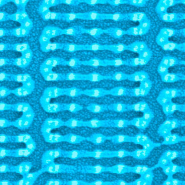 |
| MIT researchers coaxed tiny, chainlike molecules to arrange themselves into complex patterns, like this one, on a silicon chip. Previously, self-assembling molecules have required some kind of template on the chip surface — either a trench etched into the chip, or a pattern created through chemical modification. But the MIT technique instead uses sparse silicon “hitching posts.” The molecules attach themselves to the posts and spontaneously assume the desired patterns. (Image: Yeon Sik Jung and Joel Yang)
|
|
The problem is that chip features are now significantly smaller than the wavelength of the light used to make them. Manufacturers have developed various tricks to get light to produce patterns smaller than its own wavelength, but they won’t work at smaller scales.
|
|
The obvious way to continue shrinking chip features would be to use beams of electrons to transfer mask patterns to layers of photoresist. But unlike light, which can shine through a mask and expose an entire chip at once, an electron beam has to move back and forth across the surface of a chip in parallel lines, like a harvester working along rows of wheat. “It’s like the difference between writing by hand and printing a page all at once,” says Karl Berggren, the Emanuel E. Landsman Associate Professor of Electrical Engineering, who along with Caroline Ross, the Toyota Professor of Materials Science and Engineering, led the new work. The slow, precise scanning of electron-beam lithography makes it significantly more expensive than conventional optical lithography.
|
|
Hitchin’ posts
|
|
Berggren and Ross’ approach is to use electron-beam lithography sparingly, to create patterns of tiny posts on a silicon chip. They then deposit specially designed polymers — molecules in which smaller, repeating molecular units are linked into long chains — on the chip. The polymers spontaneously hitch up to the posts and arrange themselves into useful patterns.
|
|
The trick is that the polymers are “copolymers,” meaning they’re made of two different types of polymer. Berggren compares a copolymer molecule to the characters played by Robert De Niro and Charles Grodin in the movie Midnight Run, a bounty hunter and a white-collar criminal who are handcuffed together but can’t stand each other. Ross prefers a homelier analogy: “You can think of it like a piece of spaghetti joined to a piece of tagliatelle,” she says. “These two chains don’t like to mix. So given the choice, all the spaghetti ends would go here, and all the tagliatelle ends would go there, but they can’t, because they’re joined together.” In their attempts to segregate themselves, the different types of polymer chain arrange themselves into predictable patterns. By varying the length of the chains, the proportions of the two polymers, and the shape and location of the silicon hitching posts, Ross, Berggren, and their colleagues were able to produce a wide range of patterns useful in circuit design.
|
|
One of the two polymers that the MIT researchers used burns away when exposed to a plasma (an electrically charged gas), while the other, which contains silicon, turns to glass. The glass layer could serve the same purpose that a photoresist does in ordinary lithography, protecting the material beneath it while that around it is etched away.
|
|
Free expression
|
|
Dan Herr, the director of nanomanufacturing science research at the Semiconductor Research Corporation, an industry and academic research consortium, says that four or five years ago, his organization polled engineers to determine the seven fundamental shapes that self-organizing molecules would have to be able to assume in order to be useful for circuit manufacture. Since then, he says, researchers have gotten molecules to self-assemble into all seven shapes. But to do so, they’ve “changed the chemistry on the surface or etched down a trench in the surface and used that as a channel for the self-assembling process,” Herr says. Since Berggren and Ross’s technique requires no such channels to guide the self-assembling molecules, it reduces the need for electron-beam lithography. According to Herr, “That will save tremendously in terms of throughput” — that is, the efficiency with which chips can be manufactured.
|
|
Much more research is required, however, before self-assembling molecules can provide a viable means for manufacturing individual chips. Nearer term, Berggren and Ross see the technique’s being used to produce stamps that could impart nanoscale magnetic patterns to the surfaces of hard disks, or even to produce the masks used in conventional lithography: today, state-of-the art masks for a single chip require electron-beam lithography and can cost millions of dollars. In the meantime, Ross and Berggren are working to find arrangements of their nanoscale posts that will produce functioning circuits in prototype chips, and they’re trying to refine their technique to produce even smaller chip features.
|

