| Posted: April 1, 2010 |
Of Van Gogh nanotubes and nano-witches - winning nanotechnology images |
| (Nanowerk News) During the 2009 MRS Fall Meeting in Boston, MA last year, the MRS conducted the eigth installment of the popular "Science as Art" competition (View winners from past competitions). Here are the six first-place and second-place winners: |
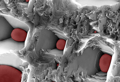 |
| Squaring the Circle The imaged object is a single crystalline diamond grain that is anisotropically etched by hot spheres of molten nickel (red). Self-organized nickel particles are obtained by sintering a thin Ni film (100 nm) that is evaporated on a polished diamond substrate. Self-organisation and etching are conducted by the following annealing procedure: 1000°C in 500 mbar H2, 24 h. (Image: Waldemar Smirnov, Fraunhofer Institut Angewandte Festkörperphysik, Germany) |
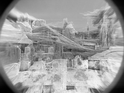 |
| SiC-SiC Composite SEM observation of a mechanical test performed on a SiC-SiC composite. (Image: Francois Willaime, CEA/Saclay, France) |
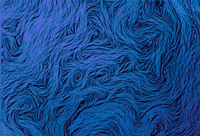 |
| Van Gogh Nanotubes From the mind of Vincent van Gogh to the surface of self-assembled arrays of carbon nanotubes. This image obtained via scanning electron microscopy, evokes the magnum opus of Vincent van Gogh, Starry Night. These arrays are formed from a dried dispersion of single wall carbon nanotubes (SWNTs) dispersed in water with a polymer PVP and a surfactant SDBS. The average width of a small SWNT bundle shown here is ∼1 µm. False color was added with Adobe Photoshop. (Image: Mariela Bravo-Sanchez, Universidad Autonoma de San Luis Potosi, Mexico) |
 |
| Dandelion Parachute Ball in the Nano-World Multiple scanning electron microscope images of boron nitride nanotubes (BNNTs) at different length scales. The BNNTs were synthesized by catalytic chemical vapor deposition (CCVD) at 1200°C. Various interesting morphologies can be formed on a Si substrate, depending on the methods of catalyst deposition. The actual diameter of the BNNTs is typically ∼50nm. (Image: Chee Huei Lee, Michigan Technological University, USA) |
 |
| Indian Summer Polycrystalline Ni-Mn-Ga magnetic shape memory alloy with a twin boundary structure (imaged with a polarized optical microscope). (Image: Claudia Hürrich, IFW Dresden, Germany) |
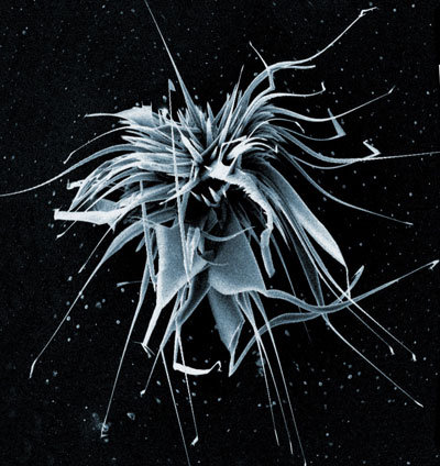 |
| Nano-Witch SEM image of crystalline wurtzite zinc oxide (ZnO) nanostructure synthesized via vapor-liquid-solid (VLS) method. (Image: Wen Hsun Tu, National Taiwan University, Taipei, Taiwan) |
We have a collection of these amazing images in some of our articles on Nanowerk. You can find the links here.
| Source: MRS |

