| Posted: April 28, 2010 |
The quantum ohm comes from PTB |
|
(Nanowerk News) With its new molecular beam epitaxy facility, PTB continues to be the only metrology institute to produce primary quantum Hall effect resistance standards.
|
|
For a long time, the electrical units are feeling at home in the quantum world. In the endeavour to trace the entire International System of Units (SI) back to natural constants, they have long been in the lead – because, among other things, the resistance can be realized with the aid of the quantum Hall effect. The Physikalisch-Technische Bundesanstalt (PTB) is the only metrology institute worldwide that can produce the respective primary standards. So that this would still be the case after the purchase of a more modern molecular beam epitaxy (MBE) facility, the scientists had to come up with some tricks.
|
|
The new facility is to primarily serve for single-electron tunnelling research – and thus, for instance, for the question of whether also the unit of current ampere can be traced back to natural constants. At first it seemed less suited to the quantum ohm. But by means of the specific alteration of the growth parameters and the layer structure of the crystals, PTB scientists succeeded in the feat of making the facility equally fit for both tasks. Thus, PTB was able to safeguard its competence to also in future be able to produce its own quantum resistance standards.
|
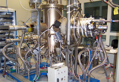 |
| The new molecular beam epitaxy facility in vertical design. Especially noticeable is the large flange-mounted cryogenic pump on the right which is responsible for the extremely good vacuum. The huge dimension of this pump can be seen in comparison to a "normal" cryogenic pump which is flange-mounted on the left and serves here only as a replacement pump.
|
|
Since 1990, the unit of resistance "ohm" has been traced back to a natural constant, i.e. the von Klitzing constant RK. Five years before, its discoverer of the same name had been awarded the Nobel Prize, because he had found out that a phenomenon already observed before (i.e. steps of constant voltage which are generated at low temperatures and strong magnetic fields vertical to a current) does not depend on a material property or the magnetic field strength, but only on the natural constants "Planck’s constant" h and "elementary charge" e. The ratio h/e2 was given the name "von Klitzing constant" and became the universal reference quantity for resistance measurements which can be exactly reproduced anywhere in the world - provided that the suitable technique and sufficient know-how are available.
|
|
The required precision measurements are rather sophisticated, as they must be performed at low temperatures of 1.4 K (also – 272 °C) and very high magnetic fields of 10 T. At PTB, the value of the von Klitzing constant can be measured up to a relative measurement uncertainty of ± 2 · 10–9, i.e. exact to nine decimals, and serves in practice for the calibration of test resistances. Starting point for these calibrations are quantum Hall primary standards which have so far been prepared at PTB in an older conventional molecular beam epitaxy(MBE) facility.
|
|
Decisive for the properties which a quantum Hall standard will have later is a so-called two-dimensional electron gas (2DEG), an ultra-thin (only approx. 10 nm in width) conducting layer in a semi-conductor layer structure of GaAs and AlGaAs. The density of the electrons must have a specific value and their mobility must not be too high. These parameters are already determined during the GaAs crystal growth - and this has for years already been successfully performed in the facility used so far.
|
|
When PTB bought a new MBE facility especially for highly mobile electron systems for additional research tasks - among other things for single electron tunneling - the question arose whether a fundamental problem could be overcome. With the facility, electron mobilities of more than 10 million cm²/Vs can be achieved and there are almost no residual impurities any more which impede the flow of the electrons. Up to now, it has not been possible to simultaneously generate low-mobility samples in such a facility.
|
|
For the investigation, quantum Hall resistances were generated in the new MBE facility at modified growth conditions: at lower temperatures and with a much smaller distance between the electron gas and the doped layer. This leads to a lower mobility without additional impurities. The values of these quantum Hall resistances were compared with the best quantum Hall standard of PTB from the conventional MBE facility. The result of the precision measurements is rather impressive, because the resistance values of the two samples agree within the excellent measurement uncertainty of ± 2 · 10–9.
|
|
The new MBE facility is, thus, regarded as validated and the supply of PTB with quantum Hall standards has been put on a wider basis. The results will be presented at the forthcoming international conference for electro-magnetic precision measurements (CPEM) which will take place from June 13 to 18, 2010, in Daejeon/ Korea.
|

