| Posted: May 11, 2010 |
High light-extraction efficiency from high-refractive-index semiconductors |
|
(Nanowerk News) Researchers at AIST succeeded in extracting light from a semiconductor into air with the highest efficiency. For this purpose, ridges were fabricated on a semiconductor surface, and then, the fabricated ridges were coated with a silicon dioxide (SiO2) layer. The mechanism of the light-extraction with high efficiency was also clarified.
|
|
Strong total internal reflection normally occurs at the interface between a semiconductor and air because the refractive index of a semiconductor material is usually far greater than that of air. For this reason, efficient extraction of the light generated in a semiconductor material into air becomes very difficult. For example, in the case of light-emitting semiconductor materials deposited on flat substrates, one can extract only a few percent of the total amount of light generated in the semiconductors (gallium arsenide (GaAs): ~2%, gallium nitride (GaN): ~4%). This serious problem hinders the improvement of the efficiency of various semiconductor optical devices such as light-emitting diodes (LEDs).
|
|
Previously, it was discovered that the aforementioned light-extraction efficiency could be significantly improved by fabricating narrow ridges on the surface of semiconductor materials. In this study, we fabricated ridges on a semiconductor surface and coated the ridges with a thin film made of a material (e.g., SiO2) whose refractive index was lower than that of the semiconductor. The light-extraction efficiency in this case was 1.5 times higher than that achieved in the previously discovered method. Our new method can be used to improve the efficiency of various semiconductor optical devices, especially LEDs, which are promising candidates for energy-efficient light sources that can be used in lighting and display applications.
|
|
The results of the present study were presented on March 20, 2010, at the 57th Spring Meeting, 2010, of the Japan Society of Applied Physics to be held at Shonan Campus, Tokai University.
|
|
Social Background of Research
|
|
High-efficiency LEDs based on compound semiconductors have attracted considerable attention because they are prospective candidates for energy-saving light sources that can be used in lighting and display applications. Research and development on energy-efficient LEDs is being intensified at the global level with the aim of popularizing LED lighting. With the widespread utilization of LEDs, the global electricity consumption would be reduced by 10% or more, and thus, in the next 20 years, energy worth approximately $120 billion would be saved.
|
|
For improving the energy-conversion efficiency of a LED, it is crucial to extract the light generated in the semiconductor into air with efficiency as high as possible. However, efficient extraction of light from the semiconductor is very difficult because the generated light tends to remain inside the semiconductor material. This is due to the strong total internal reflection (resulting from the high refractive index of semiconductor materials) at the semiconductor–air interface. While several research groups have succeeded in developing a variety of light-extraction techniques, most of the techniques have high production costs and/or poor efficiency. Thus, for the popularization of LED lighting, it is necessary to develop a high-efficiency low-cost light-extraction technique.
|
|
History of Research
|
|
In AIST, considerable effort has been devoted to the development of novel light-extraction techniques that involve the use of semiconductor nanostructures fabricated on substrates having various surface structures.
|
|
It has been demonstrated that light can be extracted into air with very high efficiency (~50%) by making use of the newly discovered evanescent wave coupling, i.e., coupling of the evanescent waves generated at small ridge structures formed on a substrate with V-shaped grooves. Two evanescent waves (a special kind of light existing only in the vicinity of the reflection interface) are generated symmetrically on the two sidewalls of a ridge upon the total reflection of light from a quantum well light-emitting layer formed beneath the flat plane at the top of the ridge (Fig. 1). This total reflection occurs at the sidewalls of the ridge. Coupling of these two evanescent waves occurs when they meet at the flat plane at the top of the ridge; the lateral width of the flat plane is smaller than the wavelength of emitted light. Consequently, the evanescent waves are efficiently transformed into light that propagate in air. In the present study, the light-extraction efficiency has been enhanced by making further improvements to this technique.
|
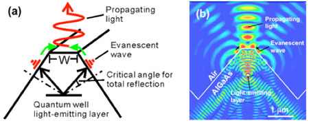 |
| Figure 1 (a) Schematic illustration of evanescent wave coupling in a small ridge structure. (b) Simulation result showing the coupling-induced efficient transformation of evanescent waves into light propagating in air.
|
|
A part of this study was financially supported by a 2009 Grant-in-Aid (No. 21360016) for Scientific Research, Scientific Research B, "Investigation on an Evanescent-to-Propagating Wave Transformation Technology Based on Pattern Substrates," of the Japan Society for the Promotion of Science.
|
|
Details of the Research
|
|
The sample used in the present study is a GaAs/aluminum gallium arsenide (AlGaAs) nanostructure grown on a GaAs substrate with V-shaped grooves by metal organic chemical vapor deposition (MOCVD). Small ridges each with a flat plane and two inclined sidewall planes are formed between two adjacent V-shaped grooves. The lateral width of the flat plane is approximately 0.5 µm. After the growth of the GaAs/AlGaAs nanostructures, a 150-nm-thick SiO2 layer is deposited on the sample surface by plasma CVD.
|
|
Photoluminescence studies revealed that after coating the sample surface with SiO2, the emission intensity of the GaAs quantum well light-emitting layer formed beneath the ridge-top flat plane was enhanced by a factor of approximately 1.7. The improvement in the emission intensity was attributed to the enhanced light-extraction efficiency due to the SiO2 layer. Similar enhancement in the photoluminescence intensity was observed when SiO2 layers with thicknesses in the range 100–600 nm were used. This enhancement was also found to occur at room temperature. By quantitative analysis of the spatial emission pattern shown in Fig. 2, we found that the light-extraction efficiency achieved with the SiO2-coated sample was at least 1.5 times higher than that achieved with the uncoated sample. Such a high efficiency in high-refractive-index semiconductor materials (refractive index > 3) such as GaAs and aluminum gallium indium phosphide (AlGaInP) cannot be achieved with conventional techniques.
|
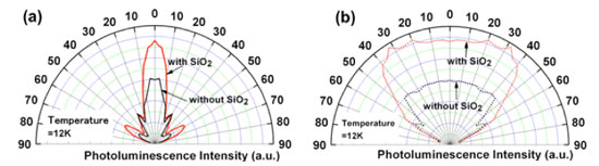 |
| Figure 2. Spatial distribution of photoluminescence intensities of samples with and without the SiO2 layer. (a) and (b) show the results obtained by performing measurements in the planes parallel and perpendicular to the V-shaped grooves, respectively. In the plane perpendicular to the V-shaped grooves, photoluminescence intensity is concentrated in the normal direction to the ridge-top flat plane.
|
|
Theoretical simulations of the electromagnetic field intensity were performed to investigate the mechanism underlying the SiO2-layer-induced enhancement of the light-extraction efficiency. In the sample coated with the SiO2 layer, evanescent waves were generated at the semiconductor–SiO2 and SiO2–air interfaces. Consequently, strong coupling of the evanescent waves occurred at the ridge-top flat plane, and thus, the amount of light that could be extracted into air was increased.
|
|
Although observed in the case of SiO2, the abovementioned phenomenon can be found in the case of other materials whose refractive index is smaller than that of the semiconductor employed. Such materials include transparent conductive materials such as Indium tin oxide (ITO) and zinc oxide (ZnO), which are widely used to form current-spreading layers in LEDs. Therefore, by using the present technique, one can achieve high light-extraction efficiency without making any significant change to conventional LED fabrication processes.
|
|
Future Schedule
|
|
The present results were obtained by carrying out photoluminescence studies on GaAs/AlGaAs-based materials. Efforts are being made to realize the enhanced light-extraction efficiency in the case of materials that are used in visible LEDs, such as AlGaInP-based and GaN-based materials, and to develop visible LEDs with ultrahigh light-extraction efficiency.
|

