| Posted: May 12, 2010 |
Micro-electromechanical systems accurately align optical components on a silicon microchip |
| (Nanowerk News) All optics research requires precise alignment of optical components to ensure that light passes efficiently from one element to the next. At the micro-scale, however, the process is much more delicate and complicated. Now, an alignment mechanism integrated onto a silicon chip to allow quick and cheap optical optimization has been demonstrated by Qingxin Zhang and co-workers from the A*STAR Institute of Microelectronics in Singapore ("A Silicon Platform With MEMS Active Alignment Function and Its Potential Application in Si-Photonics Packaging"). |
| Zhang and his team used a micro-electromechanical system (MEMS) to precisely align a laser diode made from a semiconductor, either InGaAsP or InGaAIAs, with a silicon photonic circuit. While silicon has had unrivalled success in the electronics industry, the same is not true for photonics applications owing to its poor light-emitting capacity. This means that lasers made from another type of semiconductor must be mounted onto the chip. Ensuring that such emitters line up with the silicon components often requires expensive, high-precision mechanical translation stages. “An integrated approach offers lower processing cost and higher device performance than traditional silicon–photonics packaging,” notes Zhang. |
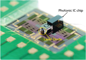 |
| Figure 1: A laser diode and a photonic integrated circuit (IC) sit on a MEMS platform. Mechanical actuators on the platform move a spherical lens so that it efficiently couples the laser light into a silicon waveguide on the IC chip. |
| MEMS are micrometer-scale mechanical actuators that move in response to thermal expansion induced by an applied voltage. “A MEMS platform can be applied to hybrid integrated silicon photonics for applications that combine both optical transmitters and transceivers,” explains Zhang. |
| He and his co-workers used two actuators to position a spherical glass lens so that it coupled the light from a near-infrared laser diode into a silicon waveguide (Fig. 1). The ball lens sat in a groove between the two actuator arms. When the arms slid in the same direction, they moved the ball left or right by up to 50 micrometers with a precision better than 0.1 micrometers. When they moved in opposite directions, the ball travelled either up or down. This gave the researchers two-axis position control of the lens. The voltage needed for this was modest at no more than 25 V. |
| Four more actuators locked the main positioning arms into place once the researchers had optimized optical coupling. They tested this pinning mechanism by subjecting their device to 2 kHz vibrations with a force equal to ten times that of gravity. The lens moved less than 0.1 micrometer. |
| According to Zhang, the next stage in the development of this technology is to control motion in a third direction: moving the lens towards or away from the laser. |
| Source: A*STAR |

