| Posted: June 22, 2010 |
Imec and partners study promising application of GeSn for future pMOS devices |
| (Nanowerk News) One promising application of GeSn would be as stressor material for Ge channels. To outperform current uniaxial compressive strained Si channel pMOSFET technology (with embedded SiGe source/drain), it will be necessary to switch to a strained Ge channel. A proposal is to use GeSn materials, which have a larger lattice parameter than Ge, as embedded source/drain stressors for Ge channels. |
| An alternative would be to implement bi-axially strained Ge grown on top of a so-called strained relaxed GeSn buffer. In addition, GeSn materials may prove also interesting for photovoltaics and optical applications. The literature predicts a direct band-gap for sufficiently high substitutional Sn concentrations. |
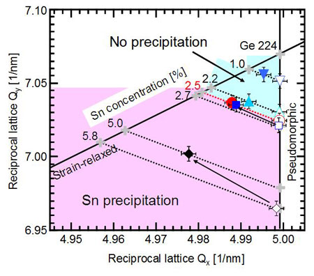 |
| Ge1-xSnx 224 reciprocal lattice points of single Ge1-xSnx layers with constant Sn content on virtual Ge substrates as measured by XRD-2DRSM. |
| Imec, the Catholic University of Leuven (Belgium) and the Nagoya University (Japan) have started a collaboration to assess the possible electrical and optical applications of this new material and to set up a strategy to solve the challenges of material implementation. Within the frame of this collaboration, imec examines the epitaxial growth and material properties of (Si)GeSn. The collaboration is supported by a joint JSPS-FWO project, which started on April 1st, 2010. (JSPS=Japan Society for the Promotion of Science, FWO=Flemish Fund for Scientific Research). |
| Simulation results show that a minimum of 5% Sn is required in the GeSn source/drain to build a strained Ge pMOSFETs that is competitive with strained Si channels. However, the Sn solubility is, in equilibrium, limited to maximum 1%. Using molecular beam epitaxy, we could already demonstrate the epitaxial growth of high quality GeSn with up to 8% substitutional Sn. Also, GeSn (with 2-8% Sn) materials have been proven to be compatible with source/drain engineering processes (B implantation and activation and NiGeSn formation). A low thermal budget has been determined for those processes on GeSn alloys: temperatures must be lower than 600°C for B activation and lower than 450°C for NiGeSn formation. |
| On May 28, 2010, the three research groups involved in the GeSn partnership have organized a workshop during which the content of this project and first exciting results were presented. First results were also presented at the ISTDM 2010 (International SiGe Technology and Device Meeting) in Stockholm and at the eMRS 2010 (European Materials Research Society) in Strasbourg. |
| Source: imec |

