| Posted: June 24, 2010 |
Depth charge: Using atomic force microscopy to study subsurface structures |
|
(Nanowerk News) Over the past couple of decades, atomic force microscopy (AFM) has emerged as a powerful tool for imaging surfaces at astonishing resolutions—fractions of a nanometer in some cases. But suppose you're more concerned with what lies below the surface? Researchers at the National Institute of Standards and Technology (NIST) have shown that under the right circumstances, surface science instruments such as the AFM can deliver valuable data about sub-surface conditions.
|
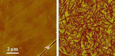 |
| Electric force microscopy can be used to detail structures well below the surface. Left, AFM height image showing the surface of a polyimide/carbon nanotube composite. Right, EFM image revealing the curved lines of subsurface nanotubes.
|
|
Their recently published ("Subsurface characterization of carbon nanotubes in polymer composites via quantitative electric force microscopy") work with colleagues from the National Aeronautics and Space Administration (NASA), National Institute of Aerospace, University of Virginia and University of Missouri could be particularly useful in the design and manufacture of nanostructured composite materials. Engineers are studying advanced materials that mix carbon nanotubes in a polymer base for a wide variety of high-performance applications because of the unique properties, such as superior strength and electrical conductance, added by the nanotubes. The material chosen by the research team as their test case, for example, is being studied by NASA for use in spacecraft actuators because it may outperform the heavier ceramics now used.
|
|
But, says NIST materials scientist Minhua Zhao, "one of the critical issues to study is how the carbon nanotubes are distributed within the composite without actually breaking the part. There are very few techniques available for this kind of non-destructive study." Zhao and his colleagues decided to try an unusual application of atomic force microscopy.
|
|
The AFM is actually a family of instruments working on the same basic principal: a delicate needle-like point hovers just above the surface to be profiled and responds to weak, atomic-level forces. A typical AFM senses so-called "van der Waals forces," very short-range forces exerted by molecules or atoms. This restricts the instrument to the surface of samples.
|
|
Instead, the team used an AFM designed to use the stronger, longer-range electrostatic force (technically an EFM), measuring the interaction between the probe tip and a charged plate beneath the composite sample. What makes it work, says Zhao, is that the nanotubes are electrical conductors with high dielectric constant (a measure of how the material affects an electric field), but the polymer is a low dielectric constant material. Such huge dielectric constant differences between nanotubes and the polymer is the key to the success of this technique, and with properly chosen voltages the nanotubes show up as finely detailed fibers dispersed below the composite's surface.
|
|
The goal, according to Zhao, is to control the process well enough to allow quantitative measurements. At present the group can discriminate different concentrations of carbon nanotubes in the polymer, determine conductive networks of the nanotubes and map electric potential distribution of the nanotubes below the surface. But the measurement is quite tricky, many factors, including probe shape and even humidity affect the electrostatic force.
|
|
The team used a specially designed probe tip and a patented, NIST-designed AFM humidity chamber.** An interesting, not yet fully understood effect, says Zhao, is that increasing the voltage between the probe and the sample at some point causes the image contrast to invert, dark regions becoming light and vice versa. The team is studying the mechanism of such contrast inversion.
|
|
"We are still optimizing this EFM technique for subsurface imaging," says Zhao. "If the depth of nanostructures located from the film surface can be determined quantitatively, this technique will be a powerful tool for nondestructive subsurface imaging of high dielectric nanostructures in a low dielectric matrix, with a broad range of applications in nanotechnology."
|

