| Posted: August 4, 2010 |
Silicon nanowires: Pressure sensors get a boost |
| (Nanowerk News) In piezoresistive materials, mechanical stress influences the movement of charge available for conduction. The application of pressure to such materials translates into an easily measurable change in conductivity, making piezoresistives ideal for use in pressure and flow sensors. Chee Chung Wong and co-workers from the A*STAR Institute of Microelectronics and Nanyang Technological University in Singapore have now demonstrated a method to increase the piezoresistive sensitivity of silicon nanowires using an applied electric field ("Electrically Controlled Giant Piezoresistance in Silicon Nanowires"). |
| Measuring the piezoresistive properties of silicon nanowires often requires the use of complicated instruments, such as atomic force microscopes, that can be used to apply stress and measure electrical properties simultaneously. Wong and his co-workers instead embedded silicon nanowires into the base of a large, 80 micrometer-long cantilever made of silicon dioxide (Fig. 1). Both the cantilever and nanowires could then be bent by a stylus, simplifying the measurement process. As a result, the researchers could combine the uniquely nanoscale piezoresistive response of the nanowires with the experimentally accessible, macroscale properties of a large cantilever without sacrificing the properties inherent to either length scale. |
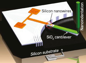 |
| Fig. 1: Schematic diagram of piezoresistive silicon nanowires embedded into the base of a large cantilever. The piezoresistance was greatly increased by the application of an electric field between the nanowires and an underlying silicon substrate. |
| The researchers also applied an electric field to their nanowires using a conducting substrate located tens of micrometers beneath the cantilever. By applying a positive voltage, they reduced the concentration of positive carriers from the cantilever and nanowires, leaving only a narrow funnel of available charge carriers near the cantilever base. This in turn greatly increased the magnitude of the piezoresistive effect on the conductivity of the nanowires. |
| As a result, the change in nanowire conductivity per unit stress increased from about a factor of 50 to over 5,000. The researchers believe the higher sensitivity may allow these hybrid nanowire–cantilever devices to be used in force-activated nanoelectromechanical switches, or hybrid mechanical–electrical logic circuits. The externally tunable sensitivity of the device may also allow for a greater degree of design flexibility. High-sensitivity switching devices could be combined with low-sensitivity conventional sensors using the same underlying device design. |
| The research was the result of a lucky coincidence, says Wong. "We discovered the giant piezoresistance effect by chance while trying to develop small-footprint pressure sensors for biomedical applications." Wong also says that real applications may soon be on hand: "Our colleagues from the Institute of Microelectronics are already integrating these nanoscale devices into flow sensors for health care applications such as catheters." |
| Source: A*STAR |

